Service hotline
+86 0755-83044319
release time:2022-04-20Author source:SlkorBrowse:6889
Today, we talk about a voltage-source PWM controller, that is, the LM5025 chip. Let's take a look at its basic parameters.
Basic characteristics:
Built-in startup bias regulator with programmable low-voltage locking output function.(UVLO),Voltage driver, 5V reference voltage,With programmable soft start function.With thermal shutdown protection function.
Input voltage at13-90V,Two packages with TSSOP16 and WSON16 can be selected.
Application scenario:
It is mainly used in various occasions related to rectifier power supply, server power supply, automobile power supply and electric energy conversion equipment to control the power output of chopping.
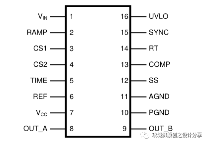
Pin distribution and definition:

(1)Power supply pin.
(2)Modulating ramp signal pin
(3)Current input detection pin of periodic current
(4)Soft-switching current sensing input pin
(5)Output overlap and dead time control pins
(6)5V reference voltage output pin
(7)Internal high-voltage regulating output, VCC voltage is regulated to 7.6V
(8)Main switching PWM output driver output pin, 3A peak.
(9) Active clamp output drive pin
(10)Power supply pin
(11)Analog ground pin
(12)Analog ground pin
(13)Pulse width modulation input pin
(14)Oscillator timing resistor pin
(15) Up and down synchronous input pins of oscillator
(16)Line undervoltage shutdown pin
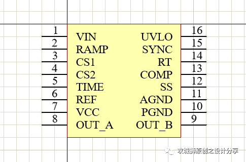
Schematic package:

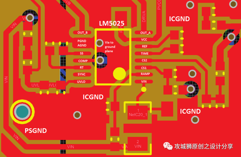
PCB package:

Design considerations:
(1)The analog ground and the power ground can be directly connected together.
(2)Bypass capacitors should be added to the power supply, and the PCB layout should be placed close to the pins.
(3)Pay attention to the pull-up and pull-down inside the chip pins, and don't destroy the pull-up and pull-down levels.
(4)The pin capacitors of CS1 and CS2 should be routed and the loop should be as short as possible.
(5)Here is a sample PCB layout. You can refer to the layout.

(This article is picked from the Internet, and opinions and opinions do not represent the position of this site. If there is infringement, please contact us to delete it!)


Site Map | 萨科微 | 金航标 | Slkor | Kinghelm
RU | FR | DE | IT | ES | PT | JA | KO | AR | TR | TH | MS | VI | MG | FA | ZH-TW | HR | BG | SD| GD | SN | SM | PS | LB | KY | KU | HAW | CO | AM | UZ | TG | SU | ST | ML | KK | NY | ZU | YO | TE | TA | SO| PA| NE | MN | MI | LA | LO | KM | KN
| JW | IG | HMN | HA | EO | CEB | BS | BN | UR | HT | KA | EU | AZ | HY | YI |MK | IS | BE | CY | GA | SW | SV | AF | FA | TR | TH | MT | HU | GL | ET | NL | DA | CS | FI | EL | HI | NO | PL | RO | CA | TL | IW | LV | ID | LT | SR | SQ | SL | UK
Copyright ©2015-2025 Shenzhen Slkor Micro Semicon Co., Ltd