Service hotline
+86 0755-83044319

release time:2022-04-01Author source:SlkorBrowse:7968
Gao Feng holds a bachelor's degree in semiconductors from Tsinghua University and a Master's degree in microelectronics from China Institute of Microelectronics. Since graduating 30 years ago, he has been working in the semiconductor industry. He has worked for Microelectronics Laboratory of Chinese Academy of Sciences, Chartered Semiconductor, TSMC America, PDF Solutions, Huahong NEC, Intergreen Chip. In 2017, I joined Shixi Capital for transformation investment. Capital partners. We are involved in more than 40 investment projects covering the entire semiconductor industry chain, from IP, EDA, materials to design, packaging and testing.
Graphic: Peak
(Set micro network report, text/Qingquan) some turning point, is the inevitable temper of life; And these hone, is the key to break the cocoon change. This has done IC design, tube fabs, dry consulting, the peak of the industry, perhaps more different feeling. Having covered almost all the key links in the semiconductor industry, Gao Feng has once again put his expertise, experience and wisdom to work to help entrepreneurs in the semiconductor industry and empower the development of China's semiconductor industry.
The road of gao Feng's life is full of many "chance coincidence", once wanted to take an examination of technical secondary school to realize the agricultural transfer, but later went to Tsinghua University; "Accidentally" I was assigned to the semiconductor major, and "accidentally" I got the qualification for postgraduate study when I did not have the chance to take the postgraduate examination. Enter the Institute of Microelectronics of the Chinese Academy of Sciences for further study, get the opportunity to study in Korea, and then open the door to the advanced semiconductor world. After work, a peak in chartered semiconductor, TSMC, huahong NEC, countersunk accumulation in the industry's top companies, from r&d to sales, "play" semiconductor industry chain after all, the peak again "encounter" investments, investors into the semiconductor industry, in the current wave of the domestic semiconductor industry, choose once again standing tide.
Seemingly a series of "chance coincidence", in fact, "efforts bear fruit", "there is no opportunity, their own initiative to attack, create opportunities; Keep learning, keep challenging, and keep pushing your boundaries." Looking back on the past, Gao Feng has deep understanding of the expression.
This plan to go up technical secondary school, but accidentally hit by accident into Tsinghua semiconductor professional
Gao Feng was born in a rural family in Fuyang, Anhui Province. His parents were private teachers and their simple requirement for their children was to read more books.
Fuyang, located in the Huaibei Plain, has a long history. It is the hometown of Guan Zhong, Bao Shuya, Lv Meng and Liu Futong. Yan Shu, Ouyang Xiu and Su Shi once served here successively. But it belongs to the populous province of Anhui, where students face enormous pressure to take the gaokao.
"At that time, our standard was that it was very good to be admitted to a technical secondary school or a junior college. As a rural child, we had to work early to solve the family burden." Gao Feng recalls the journey with deep emotion. Therefore, when Gao Feng got the second place in the high school entrance examination, he was worried that he might not be able to go to college, so he wanted to give up high school and go to secondary school directly. His chemistry teacher, who was also Gao Feng's cousin, felt sorry for gao Feng and encouraged him to go to high school and work at his parents' jobs, eventually becoming the first person to push gao Feng's fate. Peak also chose fuyang one from this, the road of life ushered in a new turning point.
Gao Feng was always among the best in high school, but he did not have a clear understanding of what he would do in the future. Gao's physics teacher recommended him to major in radio when he applied for the college entrance exam. Peak as a result, in 1985, the mistake was admitted to the department of tsinghua university radio renamed department of electronic engineering (1989), semiconductor YuRenRong weir, mega easy innovation ShuQingMing, maxscend technologies inc micro ChenHui, lattice micro li-xin zhao feng, flintlock li-dong zhao original technology such as reputation in the future, in the domestic semiconductor industry excellent characters of the lake are all his classmates, Their class became the amazing EE85 class, which contributed dozens of leading talents to China's semiconductor industry.
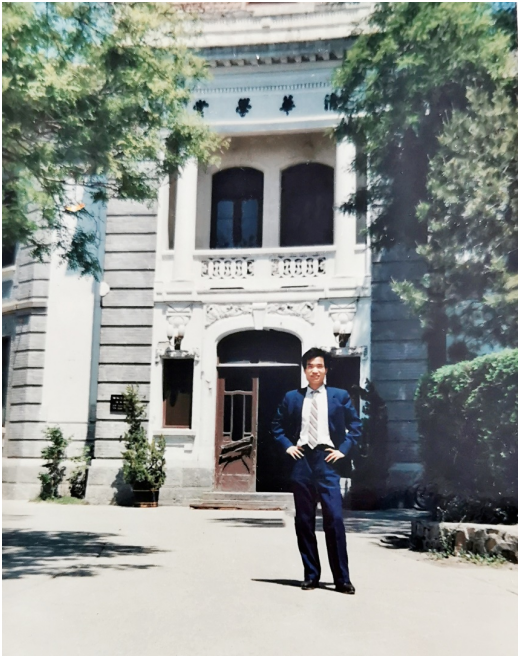
Picture: Peak in college
At that time, tsinghua Radio department was not divided into majors in the freshman year, and when it came to major two, Peak was divided into the semiconductor device physics major, which was relatively unpopular at that time. At that time, the domestic semiconductor industry was backward and we did not know much about semiconductors. When I heard it was a semiconductor, I thought I was learning how to build a radio. Gao Feng said with a smile. Although gao Feng didn't know much about this major, he had a good attitude and took it as it came, so he devoted himself to the study of semiconductor physical devices.
Recall that year's study and life, Gao Feng said: "at that time to do diode, there is not much automation equipment available, every step to design their own: with the red film to make the mask, where the light is transparent, where the light is not transparent, are hand-carved; Remove the photoresist to use acid cleaning, acid ratio, cleaning steps, how to adjust the temperature of the furnace, have to find their own hands." Although the finished products produced at that time were of different levels, he had a deeper understanding and mastery of the entire semiconductor process through hands-on learning.
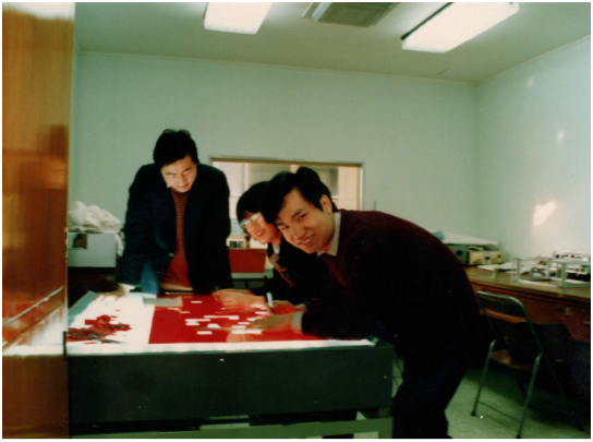
Photo: Gao Feng (first from the right) is practicing in tsinghua Institute of Microelectronics (hand-made mask)
According to the plan, gao Feng wanted to continue to take an examination of graduate students after undergaduate course, did not expect is 1989 senior year (tsinghua undergraduate is five years at that time) that year encountered a disturbance, students can not register for graduate students, gao Feng postgraduate planning can only run aground, he returned to his hometown in advance, ready to find a job in Anhui.
It was wheat harvest time and Gao Feng was helping his parents gather wheat in the field when he received a telegram from Beijing asking him to go back and apply for graduate school. Originally, although cannot enter oneself for an examination in those days, but graduate student recruit students to still continue, according to undergraduate course achievement choose an excellent admission. Due to the university four years with honours, peak "accidentally" qualification for graduate school of Chinese Academy of Sciences, to continue their education, to enter the Chinese Academy of Sciences graduate student majoring in application-specific integrated circuit design direction, the peak from the crucial device of semiconductor physics and turned into IC design field, the expansion of the knowledge of semiconductor with further exploration.
In this way, under the guidance of two teachers in junior high school and senior high school, gao Feng accidentally bumped into each other on his way to college, and tried his best to lay a solid knowledge foundation in the semiconductor major.
Learn advanced semiconductor technology and management concepts from Korea, Singapore to the United States
During his postgraduate studies, Gao Feng got an opportunity to go to South Korea for exchange and study. At the end of 1992, he came to South Korea to learn IC design at Anam Electronics Co., LTD. The design tool he used at that time was COMPASS software, but there was no such design tool in the domestic market at that time, which opened his eyes.
The learning experience broadened gao's vision and, in gao's words, "broadened his horizons", giving him a deep understanding of the leadership of foreign semiconductor development and the magical experience of applying advanced semiconductor technology to his life. After graduation, Gao Feng once wanted to engage in semiconductor design, but after comprehensive evaluation, he found that the EDA tools needed for design are very expensive, the talent is more expensive, the cost of the production of the design flow chip is almost sky-high, and the choice of OEM is very few.
Therefore, Gao Feng had the idea of going abroad for further study. After working at the Institute of Microelectronics of the Chinese Academy of Sciences for more than a year, he joined Chartered Semiconductor in Singapore in September 1994.
Chartered Semiconductor (Texas Instruments of the United States and Singapore, later acquired by Grofonde) was a rising star in the semiconductor foundry industry at that time.
Both the Singapore government and the fabs management attach great importance to talent. At CHARTERED Semiconductor, Gao Started in R&D, starting with device models, and later moved to PIE process integration, which involved several generations of advanced processes at the time, such as 0.5 micron, 0.35 micron, 0.25/0.22 micron, and 0.18 micron processes. At the time, however, chartered had an internal problem: there was a disconnect between the research and development department and the manufacturing plant, and both sides blamed each other when things went wrong. To this end, the company arranged Gao Feng to lead the R&D team into the factory to experience the mismatch between r&d and mass production and successfully eliminate the disconnect between the two. Gao Feng's ability was also recognized by the leaders, and then he was appointed as the department manager of the third franchising plant, responsible for product mass production and yield improvement.
Later, CHARTERED semiconductor successfully went public and became the third largest chip manufacturer in the world after TSMC and UMC. As for TSMC in its heyday, Gao Feng also yearned for entering the world's no. 1 foundry to learn more advanced technology and management.
So in 2001, after seven years at Chartered Semiconductor, Mr Gao joined TSMC's Eight-inch wafer factory, WaferTech LLC, in Washington state. (Eight-inch fabs were highly advanced more than 20 years ago.)
Working in WaferTech was an eye-opening experience for Gao Feng. What impressed him most was TSMC's perfect yield improvement and quality management system. In TSMC's efficient knowledge sharing system, for example, all the problems, documents and solutions related to them can be found by typing in a keyword. For enterprises with multiple fabs operating at the same time, it can be a good solution to the problem of each fabs acting independently, avoiding the inefficient situation of starting all over again.
Perfect process management and advanced technical strength ensured product yield. The project gao Feng was in charge of at that time was the technology transfer of 0.15 micron process, and 95% yield was achieved in the first transfer. TSMC's system of quality management and yield improvement really ensured service support for major customers, such as the decision to move production of Nvidia Gpus from TSMC's headquarters to its US factory, which ensured rapid and successful technology transfer.
After gaining extensive experience in yield improvement, Mr. Gao joined PDF Solutions in California. PDF Solutions is a semiconductor yield improvement solution provider, including a yield improvement consulting business and a model and data based yield testing and analysis system. There are many data analysis and statistical experts in the team, but not many people who really understand the process. One of PDF Solutions' services at the time was the production of chips for SONY's PlayStation2 game consoles, which had low yields due to complex designs such as embedded DRAM memory. To that end, Gao Feng, who understood both technology and devices, was sent to Japan to help SONY improve its profitability, and later to help Toshiba improve its profitability. Interestingly, while working at PDF Solutions, gao also helped his former employer, TSMC, increase yield on what was then the world's first 90nm process line.
From Singapore to the United States, and then to Japan, during the past 10 years, Gao Feng has traveled all over the world and major advanced semiconductor enterprises, and accumulated rich experience in semiconductor production and yield improvement, which made it natural for him to return to China to show his talents.
From engineers to sales and marketing to startup ceos, the boundaries of the workplace are expanding
In June 2000, The State Council issued "Several Policies to Encourage the Development of Software and Integrated Circuit Industry" (referred to as no.18 document), and the state approved a number of integrated circuit design industrialization bases. The semiconductor industry, which had been silent for more than ten years, finally saw the dawn and ushered in the initial stage of rapid development.
"I felt that the real semiconductor manufacturing industry should be in the mainland and the opportunity was in China." In 2004, Gao Decided to come back to Join Huahong NEC, starting from the engineering department director, engineering director, and promoted to the director of the fabs.
And these jobs, basically, continue the technical route. As Gao Feng has worked in many international semiconductor companies and has rich experience in THE United States, Japan, South Korea and Singapore, the company appointed Gao Feng to be in charge of marketing and sales.
Considering that I had been focusing on the technical field, but now I have to transform myself into the company's technical planning, market promotion and development, customer mining and other work involving face-to-face meetings with customers, frequent business negotiations and exhibition speeches, the peak of the engineer's thinking once wanted to give up.
"You're the best person. We don't look for people from outside the market." However, the leader firmly believed that Gao Feng knew both technology and factory, had done consulting, understood the situation of major manufacturers, and had abundant classmates and friends. Hence, gao Feng is "forced" to assume office hua Hong NEC market sales vice president.
Although it was another "chance coincidence", the transition to the peak of marketing and sales continued to learn and overcome challenges, and finally completed the magnificent "turn around", doing well in this position.
In the past, sales staff needed to bring a team to visit customers. When problems occurred, they had to consult technical personnel and seek collaborative support from factories. They had to hold several meetings to negotiate, resulting in low efficiency. Gaofeng can solve both orders and technical problems, bringing a new sales model to the factory.
This passive transformation not only activated the original accumulation, but also made Gao Feng start to think about the enterprise development strategy: "What I will do next year, what I will do next year, what I need, how much money I have, what is the situation of the current competitors, where is the differentiation, where is my core competitiveness..."
It is this experience and thinking that enabled him to keenly discover the future trend of the industry market development and choose the right path and lay a solid foundation for the process upgrading of Huahong NEC.
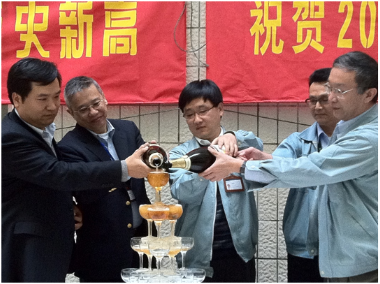
Photo: Gao Feng (first from left), then vice President of marketing and Sales, celebrating the record high shipment of Huahong NEC in the first quarter of 2011
At that time, in the field of standard CMOS technology, Huahong NEC was difficult to compete with several head OEM, Gao Feng decided that Huahong NEC market development direction to take the customized, differentiated route, with 8 inch fabs to produce discrete components. At that time, this business is mainly done by IDM manufacturers, in order to establish a differentiated production line, at the cost of increasing research and development, invest more technical force, bypass IDM manufacturers more than 1000 patents, so that Huahong NEC became the first 8-inch OEM production of discrete components. Then Gaofeng organized a cross-department team to develop a higher-end BCD process, making Huahong NEC one of the few domestic and global manufacturers capable of producing IGBT, overjunction MOSFET, SGT and other power devices and high-end BCD process. Now, many years later, huahong NEC's most profitable business is precisely the power devices and BCD technology defined by Gao Feng and his team.
Looking back, Gao Feng believes that the most important thing he gained from this experience is that it enabled him to transform from a technology-focused engineer to a marketing manager who is good at dealing with people, and also laid a foundation for his subsequent entrepreneurship.
In that year, with the opening of gem (2009) and the release of the national "New 18 document" (2011), the domestic integrated circuit industry ushered in a period of rapid development, high-tech entrepreneurial enterprises mushroomed and began to germinate, and many of the students at the peak also embarked on the road of semiconductor entrepreneurship.
In 2013, after working in Huahong NEC for 9 years, Gao Feng chose to join Integring Chip, a new company founded by his college classmates, and served as the CEO. He is committed to independent research and development of BRUShless DC motor control and drive chips to fill the gap in China. In the national Innovation and Entrepreneurship Competition that year, the Project of Intergring BRUShless DC motor control chip led by Gao Feng won the third place in the start-up group.
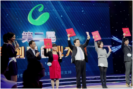
Picture: Award of the 2nd China Innovation and Entrepreneurship Competition, Intergring won the third place in the start-up group.
Gao Feng (third from right) was the CEO of Intergring
From South Korea and Singapore to the United States, Japan, and back to China, Gao Feng pursued the forefront of semiconductor development, accumulated technical experience in various industrial links, and realized the smooth transition of career roles.
Transition to investment, help semiconductor companies grow
Another "coincidence", peak "encounter" semiconductor investment.
In 2017, Zhao Yi innovation founder Zhu Yiming invited Gao Feng to join the work together, there were two work directions at that time, one is Zhu Yiming led Hefei city and Zhao Yi innovation initiated the construction of Changxin storage, the other is Zhao Yi innovation initiated the industrial investment platform Shixi capital. After a comprehensive evaluation of his ability, energy and resources, Gao Feng chose Shixi Capital as a partner to focus on investing and serving China's semiconductor industry.
"There are not many good projects in the semiconductor field, but there is a lot of money, so why should you invest in good projects?" Gao Said, "This test is the ability to empower, to be able to really help the invested enterprises, not just the problem of money."
In terms of industrial investment, The partners of Gao Feng and Stony Brook Capital adhere to three principles: the first is to focus on the semiconductor field, the second is not to invest in those who do not understand, and the third is not to invest in those who do not help, but also to help without making trouble. It seems simple, but it is not easy to do, especially the third principle.
To really help the industry, they tend not to invest in more than one company in the same niche. "If you invest in multiple companies, one of them may win, but it hurts the others," he said.
For the semiconductor entrepreneurial projects invested, Gao Feng not only invested funds, but also helped the projects to analyze market and technical problems, find production capacity for the projects, and connect upstream and downstream cooperation, which really connected superior resources and connected supply and demand. Stick to this bottom line and gradually establish positive feedback, but many projects will come to us.
A founder of a panel related business was planning to enter the semiconductor business, but he did not know how to do so, so he consulted a friend, who told him to "go to Stony Brook Capital Summit". In this way, the project leader came to me.
Knowing what was going on, Gao Told the founder bluntly: "Semiconductors are different from the panel business you did before..." But at first the founder was not happy to hear, "I do production and you tell me..." But Gaofeng felt the need to tell him. It is probably this professionalism, honesty and straight talk that finally won the cooperation of Gao Feng's Stony Brook Capital. "At that time, a lot of capital wanted to cooperate with me," the project leader later told Gao Feng. "You were the only one I actively sought out."
At the beginning of the project after the operation, the founder of peak gradually realized how important it is for a "home" in a timely manner, thank you very much for peak: "the difference is very big, really does not like panel, bad a pixel is not obvious, semiconductor risk is very big, can not do with line, one thousand has a risk, who all can not stand, must be careful and careful." Gao Feng's suggestions from company operation to product setting are convincing to customers.
Gao Feng's good reputation in the circle has won him many excellent projects. Several cases were lined up by many investment institutions, but the person in charge said, "Let them (Gao Feng team) pick the share first and give the rest to you, because their team is really supporting enterprises."
Another successful example of rapid growth due to industrial investment is peak Led Investment in a CMP equipment manufacturer. According to Gao, the key equipment in the upstream of wafer manufacturing is mainly controlled by foreign manufacturers, and it is not easy to import domestic products into the mainstream wafer manufacturing production line. That year the CMP vendor's product is wafer manufacturing companies in the trial, in foundries experience for many years, the peak can quickly judge the upstream equipment suppliers is on, the equipment can meet the needs of the fabs, the subsequent can supply and service in place, at peak and stony brook capital industry investment under the guidance and help, The equipment maker's products have since found their way into the DRAM supply chain and are receiving substantial orders.
"Help not messed up, help others is help yourself", this is a rush job for 30 years experience, relying on in the contract, consultants, startup experience and accumulation, peak laid the deep technology, market, connections, use of these resources, the peak in helping enterprises at the same time, also won a number of high-quality for stony brook capital investment projects.
Up to now, Stony Brook Capital has completed nearly 40 investment projects. According to the current listing pace, it is estimated that nearly half of the enterprises will be able to go public by 2023.
Referring to the current investment boom and high valuation in the semiconductor sector, Gao Said: "A moderate capital bubble is good for semiconductor practitioners, and everyone can make money, but excessive disorder will harm the industry. It may not be a good thing for companies that valuations are too high."
Gao Feng pointed out that for entrepreneurs, happiness comes too fast and confidence is easy to burst, but when the valuation is inflated, it will bring difficulties for subsequent financing, and investment institutions that really understand semiconductor can help will be blocked out. In addition, some high-end chip projects have a long evaluation and trial cycle, and when the product is launched, the inherent market has been divided up, limited market capacity can not support the expected sales, performance can not be realized. In addition, under high valuation, entrepreneurs are not willing to be acquired, individual champion all attack all-around champion, but the reality is that there is only one champion, these are challenges that cannot be ignored.
"If there are two or three companies listed in each segment, there is not much chance for the fourth or fifth company." Peak points out, "in order to design enterprise as an example, the present more than 2000 design companies (note: ICCAD 2021, shao-jun wei theme report chip design companies in 2021 to 2810) and finally integrated into 100 is more, I personally, there must be a next round of acquisitions mergers, time or in the next three to five years."
From the semiconductor know nothing, to plunge into the semiconductor field, a stem is more than 30 years, peak complex of semiconductor industry really reflects the "stem a line, love a line" of professional ethics. This industrial attachment even carried over to the next generation: Both of Gao Feng's sons chose to work in the fields of computer and microelectronics. The eldest is currently a doctoral student; The second undergraduate study, has obtained the doctor qualification.
As a person has much pattern has much mind. What kind of vision and mind, can see what kind of scenery. In general, peak height, now completely can choose to slow down, but the peak says: "semiconductor industry feelings make me feel, I don't have to slow down, China's semiconductor full democracy just begun, we will do stepping stones, auxiliary entrepreneurs and strivers, let more promising young company grow up quickly. Tsinghua university has a popular slogan "50 years of work for the health of the motherland", and it is a pleasure to work for me, I am willing to work together with my old and new friends in the semiconductor circle, at least until I am 80 years old!"
(proofreading/no sword core)
Disclaimer: This article is reprinted from "Qingquan", this article only represents the author's personal views, does not represent the views of Sakwei and the industry, only reprinted and shared, support the protection of intellectual property rights, reprinted please indicate the original source and author, if there is infringement, please contact us to delete.


Site Map | 萨科微 | 金航标 | Slkor | Kinghelm
RU | FR | DE | IT | ES | PT | JA | KO | AR | TR | TH | MS | VI | MG | FA | ZH-TW | HR | BG | SD| GD | SN | SM | PS | LB | KY | KU | HAW | CO | AM | UZ | TG | SU | ST | ML | KK | NY | ZU | YO | TE | TA | SO| PA| NE | MN | MI | LA | LO | KM | KN
| JW | IG | HMN | HA | EO | CEB | BS | BN | UR | HT | KA | EU | AZ | HY | YI |MK | IS | BE | CY | GA | SW | SV | AF | FA | TR | TH | MT | HU | GL | ET | NL | DA | CS | FI | EL | HI | NO | PL | RO | CA | TL | IW | LV | ID | LT | SR | SQ | SL | UK
Copyright ©2015-2025 Shenzhen Slkor Micro Semicon Co., Ltd