Service hotline
+86 0755-83044319

release time:2022-03-08Author source:SlkorBrowse:8194
Today's electronics market requires the integration of multiple high-speed functions on miniaturized printed circuit boards (PCBS) on a single board, leading designers to place wiring very close together to optimize packaging and space. This proximity can lead to unexpected coupling of electromagnetic fields, a phenomenon known as Crosstalk (see Figure 1).
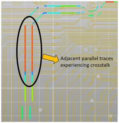
Figure 1: Graphical representation of adjacent lines on a PCB with potential crosstalk problems.
Although high-density packaging is inevitable, certain PCB design rules related to wiring on the PCB should not be violated to avoid potential crosstalk and electromagnetic interference/compatibility (EMI/EMC) issues.
(In the following sections, the phrase "critical network" refers to those high-speed clock/data lines, important sensor lines, etc., on a PCB, depending on the PCB's application.)
Rule 1: Key networks near I/O networks
It is important to look at the wiring of the critical network associated with the I/O lines, because noise can easily be coupled to the board through these I/O lines coming in and out of the PCB (see Figure 2) or carried to other boards.
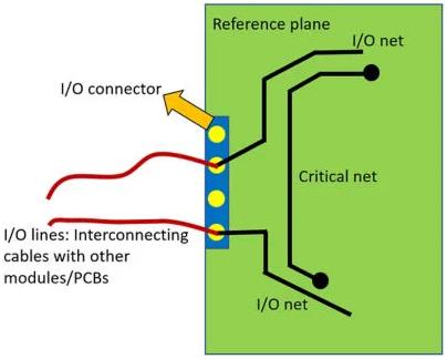
Figure 2: Schematic diagram of a scenario where the critical network and I/O network are wired close to each other.
Any noise that enters the board through the I/O line has the potential to be coupled to the critical network that carries important data/clock signals, which is basically a PCB immunity issue (Figure 3A). In a similar manner, any high-speed signals carried by the critical network can be coupled to the I/O network and eventually transmitted to the outside world and into other modules in the system via I/O lines off the board. In principle, this would be a radiation problem for the PCB (Figure 3B).
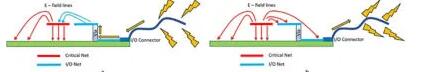
Figures 3A (left) and 3B: Potential EMI/EMC problems caused by proximity of critical and I/O networks
Rule 2: Exposed critical trace length
In short wavelength high-speed PCBS (& GT; 100MHz), the electrical length of any critical network (see figure 4a) is sufficient to make it an effective source of radiation, especially when exposed to the top or bottom layers. This unwanted radiation can be coupled to any adjacent cable, even to a cable in a device close to the cable. We recommend burying the critical network between the solid planes of the PCB's inner layer, as shown in Figure 4b. This helps to seal off the field from the line and avoid any unintended coupling in the form of crosstalk or EMI. If these critical networks have to be exposed in the outer layer, the length of the exposed portion should be as small as possible. This is because the shorter the length of the exposed wires, the less radiation they emit, because if they were electrically small, they would be inefficient antennas.
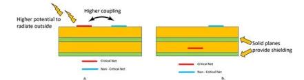
Figs. 4A (left) and B: Diagrams of exposed or closed critical networks between planes
Rule 3: Critical difference network matching
In theory, differential pairs transmit signals of equal size but opposite polarity, because the EMI produced by them cancels each other out or is negligible. However, this only works if the lines in the pair are of the same length and as close to each other as symmetrically possible. Violation of any of these can cause common mode noise and EMI problems. This is of great concern, especially for differential networks carrying high-frequency critical signals, because EMI increases the frequency of the signals carried. Figure 5 shows several examples of wiring the correct/incorrect way of critical difference pairs between the IC package and exit points (connectors) on the circuit board.
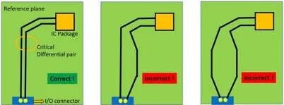
Figure 5: Return current path with split in the reference plane
Critical Difference network matching: Simulation and relation to actual test requirements
In the PCB example in Figures 6A and 6b, we have a simple case where differential pairs are wired on the PCB in two different ways: symmetric and asymmetric. In both cases, in SIwave, they are excited at one end by a differential voltage source and connected at the other end by a load.
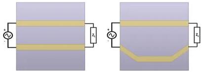
Figures 6A (left) and B: Examples of differential pairs for wiring on a PCB
We run near-field analysis in both cases. In PCBS with differential pair symmetrical wiring, the near field level is lower than in their asymmetrical wiring, as shown in Figs. 7A and 7b.
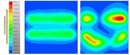
Figs. 7a (left) and B: Near field @ 597.45 MHz with symmetric and asymmetric difference pair networks
Suppose we want to test the PCB according to the EMI/EMC regulations AIS 004 (in India) or UNECE R10 (in Europe) radiant emission requirements. Figure 8 shows a comparative analysis of the simulated far field at a distance of 1 m from the PCB in the 30 MHz -- 1 GHz frequency range. Note that the case of asymmetrical difference pairs increases the emission level by about 8 to 10 dB and also results in non-compliance with 563.50 MHz and higher frequencies.
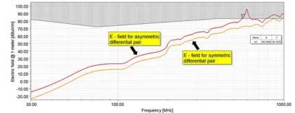
Figure 8: Comparison of 1 m radiation
SIwave's simulation at the PCB level enables early identification of such EMI problems, which can help optimize PCBS before they are designed for physical testing and even higher-level simulations.
Disclaimer: This article is reprinted from "electronic forest", this article only represents the author's personal views, does not represent the views of Sakwei and the industry, only reproduced and shared, support the protection of intellectual property rights, please indicate the original source and author, if there is infringement, please contact us to delete.


Site Map | 萨科微 | 金航标 | Slkor | Kinghelm
RU | FR | DE | IT | ES | PT | JA | KO | AR | TR | TH | MS | VI | MG | FA | ZH-TW | HR | BG | SD| GD | SN | SM | PS | LB | KY | KU | HAW | CO | AM | UZ | TG | SU | ST | ML | KK | NY | ZU | YO | TE | TA | SO| PA| NE | MN | MI | LA | LO | KM | KN
| JW | IG | HMN | HA | EO | CEB | BS | BN | UR | HT | KA | EU | AZ | HY | YI |MK | IS | BE | CY | GA | SW | SV | AF | FA | TR | TH | MT | HU | GL | ET | NL | DA | CS | FI | EL | HI | NO | PL | RO | CA | TL | IW | LV | ID | LT | SR | SQ | SL | UK
Copyright ©2015-2025 Shenzhen Slkor Micro Semicon Co., Ltd