
























服务热线


中国芯片行业的“独立团体”
2022-03-16
314
谈到半导体人才,有两所学校脱颖而出:一所是清华大学,另一所是加州大学伯克利分校。这两所学校,一所是国内的,一所是国外的,为中国芯片产业输送了大量顶尖工程师、企业家和投资者,并通过代代相传的校友关系孵化了一批又一批芯片公司。
清华大学学生朱一鸣的创业过程最生动地体现了这种校友关系:
2004年,物理系朱一鸣(89级)和半导体专业的舒庆明(85级)创办了一家芯片公司,并结识了自动化系李军(85级)。李军帮助他们获得了风险投资,并将公司介绍给了经济系薛军(83级)。
十二年后,这家名为兆易半导体(GigaDevice)的公司上市,如今市值接近100亿美元。在创立兆易半导体之前,77级半导体巨头陈大同已经创立了芯片设计公司展讯(Spreadtrum),该公司曾是联发科(MediaTek)的强劲对手。
可以说,清华大学是中国半导体领域的主力军,而这支主力军中的王牌单位无疑是“清华半导体专业”,也就是现在的清华微电子研究所。它就像《明剑》中的“独立集团”,战斗力极强。
The Institute of Microelectronics was established in 1980, and its predecessor can be traced back to the semiconductor major established by Tsinghua University in 1956. In December this year, on the occasion of the 40th anniversary of the Institute of Microelectronics, our team traveled from Shanghai to Beijing to conduct in-depth exchanges and studies at the Institute of Microelectronics. We listened to old professors’ lectures on learning and being a good person, and generations of Tsinghua Microelectronics people told their stories in the semiconductor field.
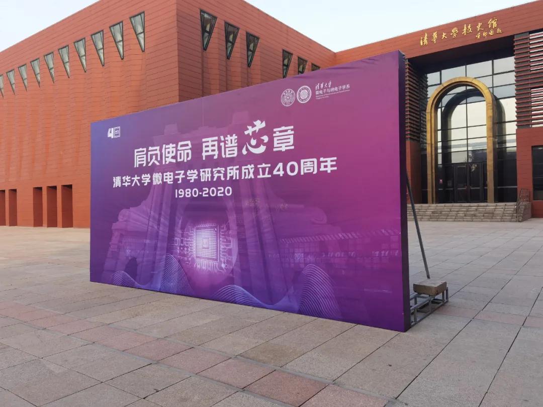
Over the past forty years, the Institute of Microelectronics has sprouted, grown, and now is full of talents, composing a majestic chapter in China's semiconductor field.
01
萌芽:人才基金会
清华微电子的最初种子是由“八位将军”和一位院士组成的。
1956年夏天,五所著名高校联合在北京大学创办了我国第一个半导体专业。清华大学派出曹培东、张建仁等八位青年教师前往观摩学习。之后,清华大学聘请了从美国普渡大学回国的王守武院士担任半导体教学科研组组长。由此,清华大学无线电工程系下属的芯片研究团队正式成立,形成了中西融合的特色。
这个教学科研小组是系里最小的,办公室位于丽寨三楼,由几间学生宿舍临时腾出的房间组成。虽然设施简陋,但研究领域却可谓“蓬勃发展”:有的从事锗器件研究,有的从事半导体收音机研究,有的从事整流器研究,有的从事光电器件研究,还有的从事硅材料研究。1959年,苏联专家切尔金前来指导后,该小组又增加了碳化硅非线性电阻器的研究。
While the field is expanding, Tsinghua is also enthusiastic about expanding its team, and even uses some "smart methods." For example, Li Zhijian, who once served as the director of microelectronics, "stuck in the Tsinghua boat".
1958年,李志坚从列宁格勒大学毕业后回到中国。他刚到北京火车站,就遇到了清华大学广播系书记李传新,李传新亲自到车站迎接他,并很快安排他到广播系工作。在计划经济时代,李志坚以为这是单位的决定,所以欣然接受了。
But after working for a while, Li Zhijian unexpectedly received a notice from the Ministry of Education, telling him that he had three places to choose from: Tsinghua University, Zhejiang University, and Xi'an Jiaotong University. Afterwards, Li Zhijian recalled that he was also surprised at the time, and was quite excited about returning to his hometown in Zhejiang and his alma mater at Zhejiang University. However, considering that he had already arrived at Tsinghua University, it was "hard to let go", so he stayed.
事实上,清华大学为了争取李志坚的邀请做了充分的准备。清华大学教授张力曾写信劝说他;1957年,包括清华大学南德恒、冯庆彦和王天珏在内的三位学者也以“无线电电子学系半导体专业预备小组”的名义写信邀请李志坚。
显然,清华大学非常重视人才。李志坚在王守武院士之后,成为教学科研团队的实际负责人,为清华微电子事业奠定了坚实的基础。
1958年,清华大学教研团队攻克了多晶硅技术的量产。同年,第一块集成电路诞生,清华大学也提出将重点发展硅集成电路。七年后,摩尔-戈登提出摩尔定律,芯片发展进入高速发展阶段。然而,即将迎来黄金时代的半导体行业却遭遇了第一次波折:文化大革命爆发后,半导体行业被一分为二,大部分人迁往绵阳,只有一小部分人留在北京的作坊里工作。
在四川绵阳的那些艰难岁月,可以说是奇迹,也是遗憾。清华人重建了实验室,恢复了教学,并与成都的970工厂开展了产学研合作。北京的半导体车间也研发出了许多产品。然而,就在同一时期,世界已经进入了大规模集成电路时代。英特尔相继推出了第一款商用内存芯片和第一款微处理器,外部世界发生了翻天覆地的变化。
After the "Cultural Revolution", the Mianyang branch was completely withdrawn to Beijing under the personal care of Comrade Deng Xiaoping. In order to catch up with the international level, the semiconductor major also ushered in a new stage: becoming independent from the Department of Radio and officially becoming an institute.
The Institute of Microelectronics of Tsinghua University, established in September 1980, has only 74 teachers and 61 students, and its funding is still insufficient. Even the construction of teaching buildings needs to be constructed and raised at the same time. But in the next forty years, the Institute of Microelectronics successively achieved breakthroughs and became the recognized Whampoa Military Academy in China's chip industry.
02
成长:突破之旅
微电子研究所的成长,就像所有青少年一样,充满了遇到的困难和取得的突破。
这些年轻学者面临的第一个十字路口是:硅还是锗。
尽管硅的物理性质优于锗,更适合半导体行业,但在20世纪50年代末,锗材料和器件已经实现大规模生产并相当成熟;而硅技术当时正处于上升期,仍处于发展初期。因此,进行锗研究时可参考和学习的资料较多,相对“安全”;而进行硅研究时可参考的资料较少,难度也更大。
Due to limited resources, everyone has indeed been arguing about this issue for some time. But in the end, a consensus was reached that we should not stop working on rectifiers, but we should also dare to look forward. Someone must study "silicon". The teaching and research team even led the students from the class of 1960 to invest in the laboratory to participate in technical research.
师生心意相通,力量足以穿透金属。20世纪60年代中期至早期,微电子研究所已经掌握了硅平面技术和硅集成电路的研发,而美国这项技术才刚刚起步不到十年。
Subsequently, the Institute of Microelectronics went through dispersion and then reunited. Just after the reunification, the Institute of Microelectronics faced a second choice: bipolar or CMOS.
当时,四川绵阳的同事负责双极型电路,北京的同事负责MOS集成电路。双方再次面临资源均等的选择。双方没有考虑各自的现有投资,而是着眼于技术发展趋势和国家利益。最终,他们再次达成共识,成立COMS,并在工艺、器件物理、电路设计和CAD技术等多个子方向上开展研究。
不久,在微电子研究所原有的教学科研实验室基础上,建成了第一条半导体超净工艺生产线;1989年,又建成了全国第一条1微米硅CMOS工艺指导线。随着新设备的到来,微电子研究所成为全国半导体院校艳羡的对象。然而,光鲜亮丽的背后,却隐藏着默默的牺牲。
当时,由于超净设备不能停机,研究所的几位核心教师像雄鹰一样轮流加班,维持生产线24小时运转。环境监测和净化设备不足,师生们只能“把毛巾折成八角”,擦拭桌椅地板,勉强保持生产线的清洁。更令人惊讶的是“如何绕过管控”。
Under the control of "Batumi" and other regulations, the equipment imported by Tsinghua University was not fully functional. The etching equipment does not have an end-point detection module, which means that the machine does not know where to pause, resulting in etching errors and wafer scrapping. Since the machine is not easy to use, researchers from the Institute of Microelectronics plan to rely on people.
我们采用“实时人工观察”的方式,通过颜色变化来判断是否达到终点,并不断积累经验以提升过程控制能力。这些故事听起来很有趣,但也发人深省,提醒我们自力更生不仅仅是一个词,更是一个艰难却正确的决定。
清华微电子克服的另一项挑战是引进光刻机。这体现了清华的国际视野,也离不开杨志连老师的努力。杨志连老师访问荷兰期间,促成了荷兰代尔夫特理工大学微电子研究所与清华大学微电子研究所的“联姻”。两所研究所随后开展了学者交流和联合培训方面的合作。这些因素促使ASML公司向清华捐赠了光刻机。
虽然设备齐全,但EDA软件仍然是一大难题。微电子研究所的许多毕业生经常前往机械工业部第一自动化研究所,使用从日本进口的制版系统和小型计算机进行电路仿真研究。他们使用的是清华大学计算机系编写的SPICE程序。虽然该软件较为简陋,但在一定程度上也为我国芯片设计EDA软件的后续发展奠定了基础。
正是凭借这种独立自主的精神和国际合作的视野,1990年,微电子率先在中国成功研制出集成1.06万个晶体管的汉字存储芯片。这标志着我国进入了超大规模集成电路(VLSI)时代,打破了“巴统”封锁。时任清华大学党委书记李传新也激动地表示:“这么少的人,这么少的钱(15万),做了这么多事,取得了这么高的成就!”
1993年启动的“金卡工程”为展现中国自主能力提供了契机。当时,中国计划在第二代证件中使用非接触式IC卡技术,但这项技术的专利基本上掌握在海外公司手中,尤其是荷兰飞利浦公司,该公司控制了90%以上的股份。
消息公布后,海外公司纷纷展开“公关活动”,希望借此获得项目。然而,法律文件涉及大量敏感信息,事关国家安全。因此,相关部门坚决提出“国内生产必须自主”。这项重要任务自然落在了清华微电子研究所等机构和企业的肩上。
Scholars from the Institute of Microelectronics led graduate students to successfully develop RFID technology and samples for simplex and duplex wireless communications from simplicity to complexity. And continuously overcome the standard elements that are higher than overseas technology. Finally, in March 2000, the Institute of Microelectronics successfully developed a second-generation IC card chip sample based on EEPROM, breaking through the patent blockade and protecting national data security.
从最初的技术壁垒到自主突破,清华微电子研究所“突破了所有障碍”,其从学术界向商业化的“核心”转型也已开启。该研究所的一批批学者已开始转型,迈入商业化阶段。
03
布鲁姆:商业传承
Since its establishment, Tsinghua Microelectronics and its sister departments have contributed three groups of entrepreneurs to China’s chip industry.
第一组是“海外光明派”,以早年赴美留学的陈大同(77级)和邓峰(81级)为代表。
上世纪1990年代,两人活跃于硅谷华人社区,分别创立了OmniVision Technology和Screen Company。颇为有趣的是,他们都是微电子领域的资深导师。清华大学长期以来秉持的“教学相长”模式,也被这两位来自北京的导师带到了硅谷。他们直接招募了许多低年级学生赴美深造,为这两家公司奠定了技术骨干基础。
昊威和Screen都是挑战全球巨头的典型创业公司。昊威由陈大同创立,利用CMOS技术击败了日本传统的CCD传感器。Screen由邓峰创立,率先将芯片硬件应用于网络安全领域,对思科产生了冲击。
短短几年内,OmniVision 和 Screen 的上市也证明了清华微电子作为一个整体有能力生产颠覆性创新产品,并在全球芯片领域占据主导地位。
The second group is the "returning to China" group, which is the first batch of entrepreneurs from Tsinghua University to return to China. Representatives include Wu Ping ('79), Feng Chenhui ('85), Shu Qingming ('85), and others.
清华微电子校友回国创业的浪潮始于2000年中国出台的新集成电路政策。自上世纪1990年代以来,清华校友在硅谷形成了一个紧密的圈子。这个圈子经常探讨潜在的创业机会,彼此之间互信度很高。随着时间的推移,许多拥有微电子背景的清华校友开始意识到在中国芯片领域创业的巨大机遇。
这一代回国创业的清华微电子专业毕业生有两个特点。
第一个特点是促进年轻人和老年人、跨行业的合作。与不同专业和年龄的校友合作创业,可以获得互补的优势和资源。
Wu Ping and Chen Datong teamed up to create Spreadtrum, starting with 2G chips; Shu Qingming and Zhu Yiming, a junior in the Department of Physics ('89), teamed up to create GigaDevice, starting from memory IP and turning to NorFlash memory manufacturing; Feng Chenhui and Xu Zhihan, a junior in the Department of Computer Science ('90), teamed up to create Zhuosheng Micro, which started with terrestrial TV chips, then switched to mobile phone RF chips, and became the industry leader.
第二个特点是它们都出现在手机电子元件市场领域,这反映了清华微电子的创业风格:选择一条大路,做实事。
展讯科技创立之初,避开了难度最高的3G芯片,首先专注于2G市场。在积累了业务基础和市场经验后,才进军3G领域。兆创科技一方面避免了闭门造车、白手起家,而是通过收购完成了存储器IP的积累。同时,它也从闪存入手,逐步拓展到NAND、DRAM等其他存储器领域。卓胜伟科技则避开了功率放大器(PA)的难题,首先研发了开关和低噪声放大器。
后续事实也证明,在半导体领域,在美国技术的压制下,创业可能需要从城市周边的农村地区开始,首先在中低端地区站稳脚跟,拥有收入和商业基础,然后再对高端产品市场产生影响。
The third group is the "local rising faction", represented by Zhao Weiguo and Yu Renrong who are level 85.
清华大学归国人员壮大了公司规模,为中国芯片产业留下了宝贵的种子。本土清华校友展现了敏锐的商业嗅觉,他们“纵横交错”地进行整合,提前开启了中国芯片企业并购的新时代。
赵卫国在紫光集团主导了展讯和RDA等大型并购交易,而余仁荣则将海外的欧米视科技纳入威信控股旗下。尽管当时中美之间并无摩擦,但双方已加快步伐,在2018年前迅速完成了多起复杂的并购交易,为中国芯片产业的整合赢得了宝贵的时间窗口。
这三代创业者各怀使命,努力前行:第一代赴美硅谷留学创业,以颠覆性创新完成对巨头的革命;第二代回国创业,在地狱般的中国市场中,找到了最适合中国国情的芯片产业链攀升之路;第三代擅长并购,在一定程度上修补行业,并利用资本加速芯片产业的初期整合。
如果再往前追溯,半导体产业的老领导也来自微电子学会。朱义伟,57级,曾任上世纪1970年代中国最大的半导体工厂——东莞光电厂副厂长,在北京集成电路产业改革中发挥了重要作用。退休后,他依然精力充沛,积极介绍在台企业家参与华京改革。
除了那些离开校园的创业者之外,事实上,微电子研究所的历任所长在学术界和商界也都是楷模。例如,前所长魏少军在本世纪初带领团队研发出SIM卡芯片,一举打破了外国芯片公司在我国的垄断地位。他本人也曾担任大唐电信技术有限公司的总裁。
The current director, Wu Huaqiang, has a double degree in materials science and management. He has served as a senior researcher at AMD and Spansion companies in the United States. In 2020, Wu Huaqiang published a paper in the magazine "Nature", realizing the first multi-array storage and computing integrated system based on memristors in the world.
过去40年来,微电子研究所培养了2,000多名本科生、1,500多名硕士生和300多名博士生。微电子研究所涉足学术、管理、商业等领域,秉承“助人、传承、引领”的传统,不断夯实中国芯片产业的基础。
04
end
At the end of the exchange, we paid a special visit to the "micro-nano processing platform" in the teaching building. There is a complete set of chip production processes here, including photolithography machines, ion implanters and other equipment, with a total value of nearly 300 million. This laboratory is completely open to undergraduate students, where they can conduct research and practical operations. Let industry enter the campus and supplement theory with practice.
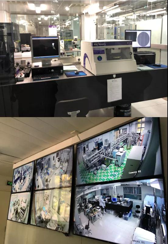
This is very valuable for Chinese semiconductors. When we talk about the semiconductor gap between China and the United States, it always falls on two aspects: time and talent. It takes time to accumulate technology, and it also takes time to patiently cultivate talents. As the saying goes, it takes ten years to cultivate trees and a hundred years to educate people.
这也是微电子研究所每位教授都在思考的问题。微电子研究所过去四十年取得了长足的进步,但仍有许多工作要做。我相信,随着一批又一批人才的成长和严谨学术精神的传承,我国自主半导体产业的发展速度必将加快,瓶颈问题也将不再困扰我们。
我们不仅要感谢微电子研究院,还要感谢全国每一位默默为中国科技突破做出贡献的学者、研究人员、工程师、企业家,乃至中小学生。我希望他们的努力能够得到回报。因为我们的独立之路依然漫长。
注:本文转载自网络,支持知识产权保护。转载请注明原出处及作者。如有侵权,请联系我们删除。
公司电话号码:+86-0755-83044319
传真:+86-0755-83975897
电子邮件:1615456225@qq.com
QQ:3518641314 李经理
QQ:332496225 邱经理
地址:深圳市龙华新区民治大道1079号展涛科技大厦C座809室
相关推荐
宋元明在华强讲座上的演讲:Kinghelm和Slkor的全球品牌之路
2026-06-05
710
两连冠之后,我们仍在进步——Slkor专访孙高飞
2026-06-11
472
数万家企业选择中国品牌——金海姆和斯尔科在全球畅销!
2026-06-24
460
射频激情,匠人之路:三十余载的坚定奉献——金海姆首席工程师秦宏祥先生访谈录
2026-06-26
523
明年见!| Slkor 出席 2026 年中国电子音乐节精彩回顾
2026-07-14
232





 粤公网安备44030002007346号