
























服务热线


中国先进封装和检测产业及设备的“集体崛起”离不开中国的重要保障
2022-03-16
380
1958年,德州仪器(TI)的杰克·S·基尔比(Jack S. Kilby)利用锗(Ge)衬底将多个晶体管、电阻器和电容器连接起来,成功研制出世界上第一个集成电路。随后,罗伯特·诺伊斯(Robert Noyce)发明了基于硅(Si)的集成电路。如今,大多数半导体应用都是基于硅的集成电路(即所谓的第一代半导体)。芯片已成为现代工业的“石油”。
芯片行业初期完全采用IDM(集成器件制造)模式。英特尔和德州仪器既设计又制造芯片,这使得小型公司很难涉足芯片行业。
张忠谋曾就职于德州仪器(TI),于1987年创立了专业的晶圆代工企业台积电(TSMC),其“解耦”模式开启了半导体代工的新时代。芯片制造分为设计、晶圆制造和封装测试三个阶段。设计公司(无晶圆设计,Fabless模式)可以将晶圆制造、封装测试等环节外包,专注于设计、销售和服务。
科技老手戴辉:我一直想分享一件往事,今天终于有机会了。早在1993年,王祥福老师就带我们班去无锡实习,在流水线上手工焊接电路板。每天早晚,我都会看到一个高墙环绕、戒备森严的大院,院子里一块大牌子上赫然写着“华京”两个大字。当时我还很纳闷,这是做什么用的。原来,908工程的5英寸3微米生产线正在如火如荼地建设中。
台湾的芯片外包半导体组装及测试产业(OSAT,外包半导体组装及测试)发展迅速。日月光(ASE)和硅片(Silicon Products)均成立于1984年。
无数轻资产芯片设计公司应运而生,例如著名的高通和英伟达,中国大陆在芯片设计领域也取得了长足进步。1991年,联想的倪光南就开始制作芯片,华为的徐文伟也制作芯片(由德州仪器代工)。1993年,国威成立,成为深圳芯片产业的“黄埔军校”。目前,中国大陆有数千家芯片设计公司(有人说是数万家)。
当然,资产密集型IDM模式一直存在,两种模式各有优势。AMD成功地从IDM模式转型为FABLESS模式,而英特尔则一直坚持IDM模式,近期升级到IDM2.0模式,大力投资先进封装技术并重返晶圆代工市场。
The closed beta process is "hidden in the boudoir" and is unfamiliar to the public. In fact, packaging and testing can be independent and can be done in one factory or in different factories. The packaging and testing adopts the business model of "processing with supplied materials", and orders come from semiconductor design manufacturers.
Traditional chip-scale packaging is to seal the die after cutting the wafer into a closed space (casing) to protect it from the influence of the external environment, impurities and physical forces. At the same time, the corresponding pins (or pins) are drawn out, and finally used as a basic component.
晶圆级封装技术(Wafer Level Packaging)是一种将整个晶圆封装并进行测试,然后切割成单个成品芯片的技术。封装后的芯片尺寸与裸芯片的尺寸相同。
集成电路测试采用多种方法来检测不合格的芯片样品。它主要分为两个阶段:一是封装前的晶圆测试;二是封装后的成品集成电路测试。目前,封装阶段也引入了目视检测。
我在2021年中国国际半导体展(SEMICON CHINA 2021)上最直观的感受是,中国大陆的封装测试行业正在蓬勃发展,带动了设备和材料集团的崛起。许多类别的设备都有国产机型,例如中科飞驰、普莱森、雷明激光、硅能、跃信、加速、宏泰、宏邦、奥克塔维亚理想等众多厂商的产品。目前,国产设备的市场份额仍然很小,未来发展空间巨大。
当然,封装和测试技术也应用于全芯片领域(例如电阻器、电容器、电感器、LED、显示器和太阳能多晶硅等分立元件),但本文不作赘述。新奇微封装专注于PCB、显示器(FPD)及其他领域。
一,大陆Packaging and testing industry: booming20年份
目前,全球十大半导体封装测试厂商主要包括:台湾日月光半导体(不包括硅业和USI)、美国安靠、大陆昌电科技、台湾硅业、台湾力成半导体、大陆同福微电子、大陆华天科技、新加坡联合测试、台湾KYEC无线电和台湾新邦科技。其中,大陆“三剑客”昌电科技、同福微电子和华天科技均位列前十。
During the semiconductor industry construction boom in the past two or three years, hundreds of mainland companies have entered the packaging and testing field. Mainland China's overall share of the global packaging and testing industry is getting higher and higher, and will exceed 50%.Even Foxconn has entered the packaging field. This number is similar to China’s global share of PCB (Printed Circuit Board) bare board and SMT (Surface Mount) production capacity. There are more than 30,000 SMT production lines in mainland China, accounting for more than half of the world's total. There was once a joke: If there is a traffic jam in Dongguan, the price of electronic products around the world will fluctuate.
人们普遍认为,中国大陆封装测试企业的水平已基本与国际先进水平接轨。大陆半导体有望率先在封装测试行业实现全方位领先全球。
预计整机制造行业使用的芯片将主要在中国大陆进行封装;在中国大陆封装的芯片也正大规模出口到越南/印度等新兴的整机制造(SMT)市场。
换句话说,如果中国大陆不发展包装产业,未来部分SMT产能转移后,中国大陆在电子供应链中的核心地位将会被削弱。
值得指出的是,包装设备和材料的供应链已实现国际多元化,在欧洲、美国、日本和台湾地区积累了深厚的资源。
中国大陆大力发展包装和测试行业,这不仅提高了全球产能,也降低了电子产品的成本,为世界各地的人们带来了利益。
The development of mainland China's packaging industry has the following key nodes.
1. 2000年前后,江苏南部作为中心,大规模进入现代包装产业
Before 2000, it was mainly in the traditional packaging stage. After that, advanced packaging developed rapidly, and mainland China had the opportunity to catch up and surpass it.
产业发展的总体逻辑是:中国庞大的电子产品消费市场和丰富的劳动力资源驱动着电子产业的发展。外资芯片公司通常将芯片封装和测试环节外包给中国大陆,然后再直接运往整机工厂。例如,AMD在苏州的封装厂就与苏州工业园区的PC主板制造产业紧密相关。
如果没有整个机械行业的驱动,芯片就无法制造。这一点对我来说非常重要,因为我本身就拥有完整的机械行业背景。
中国大陆的先进封装产业基地位于江苏南部,这里拥有得天独厚的时机、地域和人才优势。它毗邻苏州工业园区、上海的ODM/IDH企业(如华勤、闻泰、龙奇等)以及张江众多芯片设计公司。
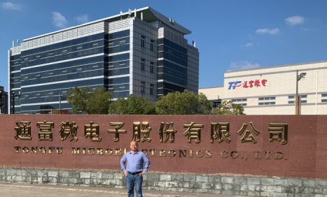
The three major packaging and testing companies, Tongfu Micro (joint venture in 1997), Changdian (restructured in 2000), and Gansu Huatian (established in 2003), were all developed based on early electronic discrete component factories.
硅产品公司于2002年底在苏州工业园区成立了硅产品技术(苏州)有限公司。日月光半导体公司自2002年起在上海张江高新技术产业园投资建厂。京方科技公司于2005年6月在苏州成立,其技术源自以色列。
2. Self-designed copycat GSM mobile phones have brought about great development in mainland China’s chip design industry and also driven the packaging industry.
2000年,中国GSM移动用户数量翻了一番,超过100亿,成为全球最大的手机市场。诺基亚在东莞的手机工厂和三星在惠州的工厂规模都很大,本土手机品牌也开始发展壮大。
Starting in 2006, with the enhancement of global GSM coverage (changing the misunderstanding that 3G will replace GSM), a wave of self-designed white-brand GSM mobile phones broke out.
Mainland China's local chip design industry has also experienced its first major explosion, which has also given a great boost to advanced packaging.
Du Zheng, CEO of Corestar, who once worked at Howe, said that CIS (CMOS image sensor) has requirements for wafers, packaging, and testing, and requires the entire process to achieve good quality.
Jingfang introduced packaging technology from Israel, and Howey also participated in the investment. 70% of the packaging production capacity of Jingfang and Huatian Kunshan factories was once only served by Gekko Micro's CIS.
至于测试方面,CIS产品也发生了变革。
格科威早期图像传感器的图像质量检测必须依靠人眼判断。随着白标GSM手机市场的快速扩张,格科威这家最初以极具性价比的CIS(低至100,000万像素)起家的公司不断发展壮大,多次迁至张江展馆,主要用于测试,展馆里总是挤满了年轻女孩。
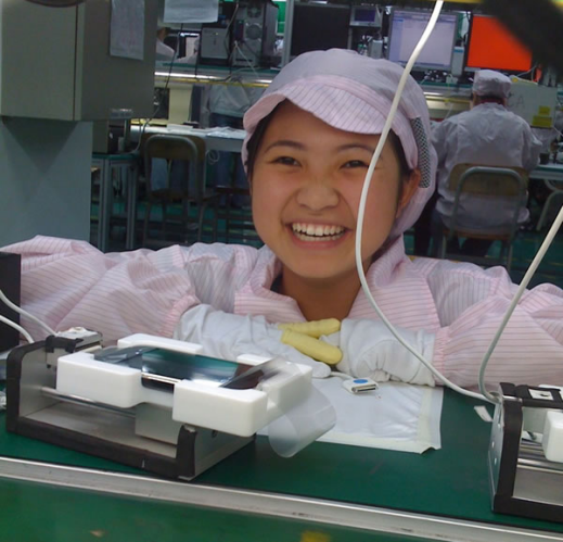
注:iPhone早期,其相机功能是手动测试的。图片展示的是2008年的“iPhone女孩”。
随着自动化和人工智能的发展,杜正介绍说,现在有了功能强大的自动化设备(搬运器)和人工智能检测方法。封装公司同福微电子的苗晓勇先生介绍说,该公司与新世达在晶圆级芯片封装(WLCSP)工艺方面开展合作。该工艺将芯片级封装(CSP)和晶圆级封装(WLP)集成在一起,使芯片具有“短、轻、薄”的特点,符合消费电子产品向智能化和小型化发展趋势。
吉维网创始人老尧(王彦辉)2007年也曾测试过小型设备,但后来发现自己更擅长媒体工作,不过他一直关注着这个行业。他说:很多芯片设计公司都会自行采购/选择测试设备,并将其放在测试生产线上。
巧合的是,苹果公司在其生产线上也采用了同样的做法。
一二014 years later, global packaging companies have consolidated, and Chinese companies have used mergers and acquisitions to enter advanced packaging and gain major customers.
昌电科技收购了新加坡的 STATS ChipPAC,同福微电子收购了 AMD 的苏州和彭州封装测试厂,华天科技收购了美国的 FCI 和 Unisem 公司,京方科技收购了智瑞达和 Anteryon 公司等等。
人工智能发展迅猛,AMD 的利润飙升,苏的母亲(苏子峰)笑得合不拢嘴,同福也随之崛起。
4. 深圳存储带动存储封装技术的快速发展
华强北是中国最早的专业电子产品市场。电脑内存条也是机械市场最热门的产品之一。深圳内存也正是在这里起家的。
2014年,随着智能手机和移动互联网(以微信为代表)的发展,存储需求也大幅增长,尤其是照片存储,手机128G的存储空间已经不够用了。2018年,全球半导体产业规模达到476.7亿美元。其中,存储器作为最大的半导体品类,占半导体市场近35%的份额。同年,中国大陆进口集成电路约310亿美元,其中约100亿美元为存储器。长江存储和合肥长信在中国大陆均拥有自己的晶圆厂。
中国大陆品牌内存的增长潜力非常巨大。深圳一带聚集了众多优秀的内存品牌企业,例如近铁、创新科技、宏碁、龙科、记忆、百威、嘉和金威(排名不分先后)。深圳科技(收购了金士顿的Payton品牌)和康佳也已进入市场。这些企业都涉足芯片封装和模块封装领域。
受深圳对存储器需求的推动,太极半导体、昌电科技、同福微电子等公司也在努力开发存储器封装和测试技术。
这里还有一个关于国产设备驱动的故事。2013年,深圳凯艺科技有限公司(一家为电子制造业提供制造技术解决方案的公司)的存储客户提出了对封装自动化检测的需求。凯艺曾联系韩国和日本的供应商开发相关产品,但由于测量精度要求高、软件算法复杂而被拒绝。最终,他们与本土制造商深圳奥克塔维亚(Octavia)合作。奥克塔维亚将其成熟的SMT技术移植到封装工艺中,实现了在线连续视觉检测。该检测系统于2015年开始上线,并应用于存储、传感器封装等产品。
5. 人工智能物联网和电动汽车推动了先进封装技术的新一轮增长
At the SEMICON CHINA 2021 exhibition, it can be seen that advanced packaging and high-density packaging are developing rapidly.
随着人工智能物联网时代的到来,喝茶(自动加水烧水)、吸烟(电子烟)、开门(智能锁)、扫地(机器人)、在家学习(笔记本电脑)等都配备了大量的芯片。
特斯拉在临港建厂。中国已启动新的基础设施建设,并建成充电桩,电动汽车和两轮电动车产业蓬勃发展,对芯片的需求也随之激增。车规级芯片对可靠性要求高,封装也有特殊要求。
The packaging industry is experiencing explosive growth in China, with many companies pouring in. Ningbo took action. The newly established Yongsi Electronics directly positioned itself for advanced packaging and entered the ranks of giants with rapid progress. It is said that it is already ranked very high in the country.
2. 中国大陆封装和测试技术的发展:电子行业无法绕开中国
以手机为核心的电子产品是中国最大的出口产品,其次是纺织品。你还记得改革开放初期用一亿条裤子换一架飞机的笑话吗?
从宏观角度来看,全球抗击疫情离不开电子产品;从微观角度来看,很多人洗澡时都会拿着手机!
电子信息技术产品的供应链非常复杂。众多的零部件、复杂的软硬件设计以及工艺要求,都清晰地体现了中国的工程红利和制造红利。因此,这是最难与中国脱钩的行业。即使实现了“去全球化”,也无法实现“去中国化”。
电子产品的生产过程大致分为三个部分:晶圆制造、封装和整机制造(SMT表面贴装是核心)。晶圆连接到封装测试,整机制造则连接到晶圆制造的底部。
尽管晶圆行业从业人员不多,但技术要素却牢牢掌握在西方手中,差距显而易见。要彻底解决“卡颈”问题,还有很长的路要走。值得注意的是,美国正在大力发展晶圆制造领域。台积电、三星、英特尔和格罗方德等公司将大力发展采用美国最先进工艺的晶圆制造技术。
印度每年销售一亿到两亿部手机,当然必须发展制造业。中国大陆的整机制造必然会将部分生产转移到海外(例如,苹果、小米等公司已经在印度拥有生产能力)。
Therefore, from a strategic point of view, it is necessary to strengthen the upstream chip packaging and testing field. Only in this way can China still occupy an important link in the supply chain and ensure that the overall core position of "Made in China" remains unchanged.
南京邮电大学南通包装研究所的蔡志匡教授动情地表示,最近人们对包装最大的感受就是“闻了闻颜色就变了”。例如,在BGA包装生产线上,如果BGA基材产能不足,他们不敢贸然接单。国家应该加大投入,尽快从“闻了闻颜色就变了”的阶段过渡到“闻了闻颜色就变了”的阶段,让每个人都有基材,每个家庭都有生产能力。
This time, as soon as I entered the SEMICON exhibition hall, I bumped into the booths of Shennan Circuit and Tianxin Interconnect. One hand was making packaging substrates, and the other was making advanced packaging.
Jiwei.com’s article tells the reasons behind it: Behind the serious shortage of packaging substrates: upstream materials and equipment have become a bottleneck for production expansion
引线框架也是一种重要的封装材料,但其生产能力也不足。
在线设计公司“急需产能”这一说法并非空穴来风。
3. Advanced packaging: combined with wafer and SMT
1先进的包装也是高科技。
在半导体产业发展的早期阶段,半导体封装一直被视为技术门槛相对较低、劳动力成本相对较高的行业。封装是集成电路产业链中最难盈利的环节,需要不断增加投资才能获得每一美元边际收益。
As the integration level of chips increases, the technical requirements for semiconductor packaging are getting higher and higher, which makes semiconductor packaging no longer a simple technology. All kinds of advanced packaging and new processes have appeared, which makes me dazzled.
As packaging complexity continues to increase, advanced packaging has become an important source of production increment. In the future, the ratio of the three sections of the chip is expected to be: 3 (design): 4 (wafer): 3 (packaging).
Traditional packaging passively accepts the arrangements of chip design companies. The current trend is that chip design manufacturers increasingly need to conduct collaborative design with packaging manufacturers. In the post-Moore era, chip back-end manufacturing technology will drive the development of chips towards high performance and high density.
At the 2019 Jiwei Semiconductor Summit, Dad Jiang (Jiang Shangyi) believed that the semiconductor industry environment has undergone tremendous changes. This is mainly reflected in the following aspects: First, the progress of Moore's Law has approached the physical limit, and the most advanced silicon processes (such as 7nm, 5nm) can only be used by a very small number of extremely high-demand products (such as mobile phone main chips); second, the progress of packaging and circuit board technology is relatively backward, gradually becoming a bottleneck for system performance; third, the era of chip (design company) diversification is coming, and the market will no longer be in the hands of a few manufacturers. According to different systems and the special needs of each unit, selecting appropriate units and reintegrating them through advanced packaging and circuit board technology will be one of the development trends in the post-Moore era.
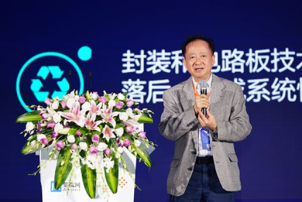
昌电科技CEO郑力表示:“如今的半导体封装不仅仅是将芯片密封到外壳中,还需要对内部芯片、芯片布线、互连接口等数十道工序进行处理,甚至还需要对晶圆进行重新排列。之后,一些芯片还需要进行布局,并与其他封装内的芯片互连,有时甚至需要进行其他工序。不仅如此,这些芯片还需要高密度连接,才能使各个功能模块协同工作。因此,在后摩尔定律时代,封装不再仅仅关注线宽、线间距和集成尺寸,而是更多地关注如何提升系统性能以及如何提高整个微系统的集成度。”
2、Combination of packaging and front-end wafer manufacturing
令人震惊的消息是:台积电、中芯国际等晶圆厂也已进军晶圆级封装行业。起初我认为这对封装行业构成威胁,但常电CEO郑力认为这实际上是一件好事。晶圆级封装(WLP)是先进封装技术的发展路径之一。如果晶圆级封装继续向二维、二维半、三维等多维方向发展,必然会与晶圆厂展开合作。这是因为晶圆厂具备在晶圆上进行硅通孔(TSV)工艺制造的能力。对于硅传输板而言,晶圆厂还可以制造硅中介层(硅中介层),这是一种带有高密度布线的晶圆。封装测试厂需要进行晶圆重排(RDL)工艺,然后在封装测试层面将这些布线重新高密度地集成到晶圆上。
业内专家指出,昌电和日月光在高端封装测试的良率方面存在约10%的差距,这需要时间才能弥补。但可以预见的是,大陆封装测试的起飞速度可能比前一阶段的晶圆制造更快。将封闭测试视为后端已不再是过去的做法。如今,封闭测试与前端之间存在诸多交集。挑战无处不在,需要坚持不懈和耐心!
3, advanced packaging and SMT surface mount combination
In addition to the integration with wafer manufacturing described above, packaging and testing is also closely integrated with complete machine manufacturing (SMT as the core).
Around 2015, I saw the demo of a multi-chip package for the first time, integrating the required components into a module, reducing the number of packaging and wiring problems, saving space, improving performance, and reducing the cost of the entire machine.
系统级封装 (SiP) 和表面贴装 (SMT) 密不可分。ASM-PT、K&S 等主要设备制造商最初都是 SMT 贴片机的制造商。SiP 可以减少芯片系统集成过程中面临的工艺兼容性、信号混叠、噪声干扰和电磁干扰等问题。
手机射频前端模块(PAMiD等)大多采用SiP或类似工艺。凯源通信的贾斌表示,随着5G的普及,越来越多的射频元件被引入手机。如果将它们单独封装,然后再贴片到PCB板上,手机可能无法容纳,因此最好进行集成。SAW、BAW、PA、LNA和RF开关等射频芯片的基本工艺各不相同,无法采用SoC解决方案。相反,可以使用系统级封装等工艺将多个芯片封装成模块。国际知名厂商天工、Qorvo、Avago(被博通收购)、高通等都在这样做。我在网上搜索了一下,发现射频工艺有很多种,例如GaAs、体硅CMOS、SOI绝缘衬底硅、硅基MEMS、SiGe硅锗等。
摄像头模块和指纹识别模块均采用COB(芯片封装)技术。芯片未经封装,直接切割成裸晶圆(芯片),将键合和其他封装工艺推迟到模块阶段进行。
常见的“牛粪芯片”也采用COB工艺。裸芯片通过键合设备固定在PCB电路板上,然后滴上环氧树脂胶。之后,其他元器件通过SMT工艺贴装上去,电路板就完成了。这就是来电显示电话控制板的工作原理。图中金色的圆圈是围绕芯片的众多键合金线。
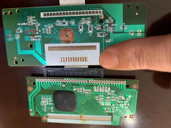
注:CID电话控制面板(作者戴辉在天迅龙拍摄)
4. 先进封装:专利纠纷
专利战在封装领域也不可避免地会发生。吉维旺知识产权咨询业务负责人马克先生讲述了一个典型的中外企业围绕封装专利展开的诉讼案例,该案例源于MEMS麦克风行业。
美国公司 Knowles 是第一个将 MEMS 技术应用于麦克风制造以取代传统驻极体麦克风的公司,该公司于 2000 年申请了一项基础封装专利。基于这项专利,Knowles 于 2006 年对美国 Akustica、新加坡 Memstech、美国 ADI、英国 Wolfson、韩国 Baoxing、美国 Amkor 和中国大陆歌尔科技提起了专利侵权诉讼,甚至还启动了 337 调查。
中国大陆的MEMS麦克风制造商AAC早期就与Knowles公司签署了专利许可协议,以避免专利诉讼。然而,高昂的专利许可费也成为大陆企业不得不面对的现实。相比之下,台湾的产业链则更注重规避Knowles的美国专利。在台湾工业研究院的领导下,联合美路等主要电声厂商,至少有七项专利围绕Knowles的封装专利展开规避。然而,正是由于过度强调规避Knowles的基础专利,台湾原本在半导体制造领域的优势未能充分发挥到MEMS麦克风领域,错失了市场机遇,最终沦为中国大陆的AAC和歌尔科技。
五,seal up类型设备:"The Rise of the Group"
我亲眼见证了电话和程序控制交换机、移动通信和移动电话产业集团的崛起,也促成了大陆芯片产业集团的崛起。“集团崛起”一词用来形容封装和测试设备行业最为贴切。
At SEMICONChina 2021, I saw the localization of many categories of packaging and testing equipment. Packaging includes grinding, cutting (DICING), DIE BOND (crystal bonding), WIRE BOND (wire bonding) and other main equipment areas.
The development of domestic equipment will be very helpful in dismantling monopoly, reducing costs, improving performance and improving efficiency.
在2020年天水包装大会上,华天晓胜利表示,包装和检测企业应坚持合作而非竞争的理念,积极培育国产设备和材料,逐步完善检测平台。
Using domestic equipment to break the monopoly of Western equipment can effectively reduce costs, which is obvious in packaging.
新奇微电子刚刚在科创板上市,填补了国内无掩模光刻设备市场的空白。其直写式光刻设备服务于PCB(印刷电路板)和全半导体(FPD显示器)领域,并计划推出用于晶圆级封装(WLP)的直写式光刻设备。上市后,该公司股价飙升,整个半导体行业也随之上涨(希望不仅仅是反弹)。
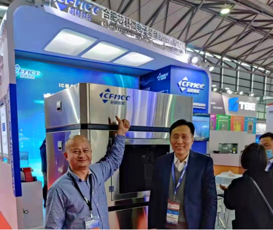
注:作者戴辉和新奇微电子首席科学家曲璐杰在展位上
在芯片键合机方面,东莞普莱森曾填补了国内线性IC级芯片键合机(DIE BOND)的空白。
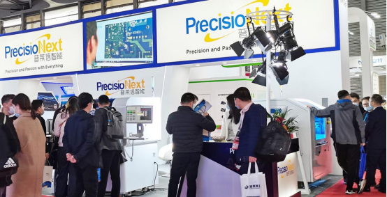
来自 Beyond Moore Fund 的王林贡献了一个案例:雷鸣激光推出了性能可与西方公司媲美的激光开槽+激光暗切设备,打破了市场垄断。
6. Test Equipment: “The Rise of Groups”
The testing equipment mainly includes the sorting machine Handler for chip-level testing, the probe station Probe for wafer-level testing, and the automatic testing machine ATE.
测试设备的本地化具有巨大的发展潜力。新的工艺流程带来了定制化需求,而采用国产设备可以一步到位地实现更高的效率和更好的性能。
深圳硅电是一家生产探针台和分拣机的制造商。
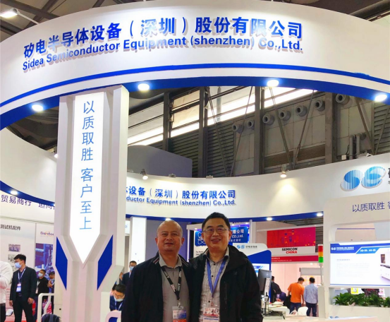
注:作者戴辉和哈尔滨工业大学胡宏教授在硅胶展位
Zhang Yue, CEO of Yuexin Technology, introduced me to the main product Memory memory testing equipment, which has done a lot of work on high efficiency, consistency, and stability.
Accelerate Technology推出高性能ATE自动测试机,结合人工智能技术。
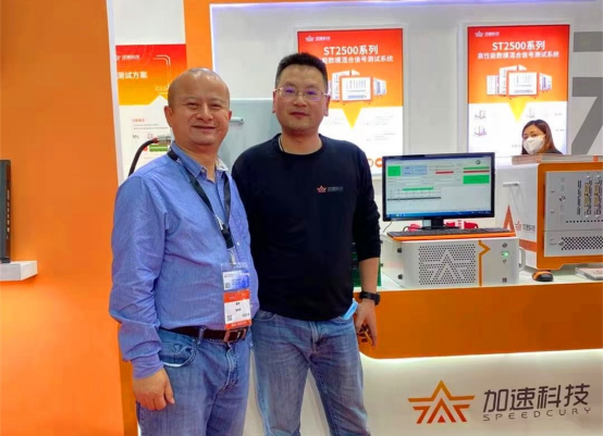
Note: Author Dai Hui and Acceleration Technology CEO Wu Gang at the booth
绍兴宏邦展示了各种功率器件测试设备和分拣机。我“撸起袖子”亲自试用了一下。
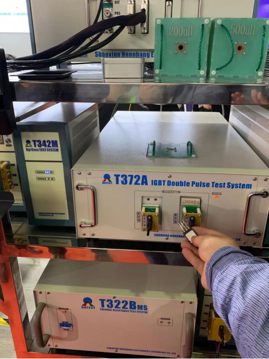
注:绍兴鸿邦展出的分立器件测试机
南京宏泰半导体展示了一系列半导体ATE自动化测试产品。该公司于2019年全资收购了以模拟测试技术闻名的日本Azurtest株式会社(Azurtest)。
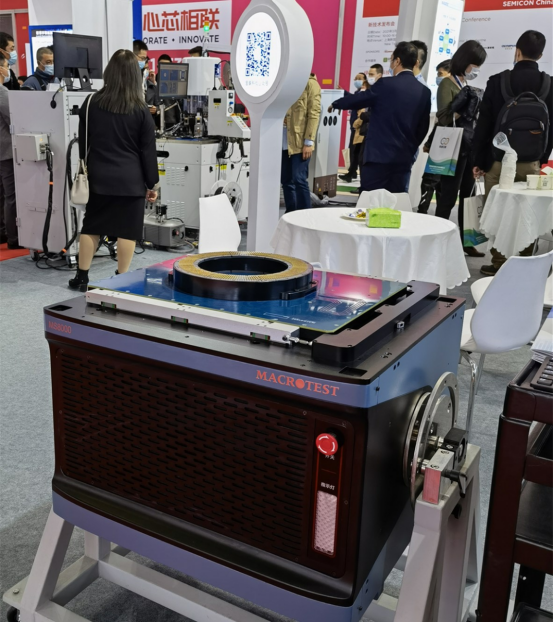
注:宏泰半导体展出混合信号测试机MS8000
相关服务公司也在发展壮大。上海吉峰电子提供材料分析、故障分析和可靠性认证等服务。
七,包装材料:steady development
在材料领域,中国大陆也在迎头赶上,例如最近“讨论过基材和引线框架的底色变化”。
The electronics industry uses a large amount of precious metal gold, mainly in wire bonding of packages. The industry continues to promote the use of copper (or even aluminum) to replace gold in more and more scenarios, and mainland companies have also done a lot of work.
Shenzhen's chip manufacturing industry is slower than some domestic cities, so it plans to overtake in corners. Starting in 2020, Shenzhen will promote the development of a new generation of information and communication technology. Bi Yalei, secretary-general of the Shenzhen Robot Association, said that on December 30, 2020, the Advanced Academy of Sciences of the Chinese Academy of Sciences established the Shenzhen International Innovation Institute of Advanced Electronic Materials (hereinafter referred to as the "Electronic Materials Institute") in Bao'an, focusing on high-end advanced electronic packaging materials and aiming to promote the localization of high-end electronic materials to "break through."
8. 真正的“核心”英雄:不要忘记最初的“核心”,并积累数千英里的硅片。
国家集成电路基金负责人丁文武先生发布了一首歌曲《真正的“芯片”英雄》,唱出了许多芯片人的“核心”心声:用我们的“核心”共同实现中国的“核心梦想”;让我们的“核心”像星海一样,让世界互联互通。
Disclaimer: This article is reproduced from "Dai Hui Steve", which supports the protection of intellectual property rights. Please indicate the original source and author when reprinting. If there is any infringement, please contact us to delete it.
相关推荐
云帆瑞达李刚专访:毫米波雷达产品的精准性与人文关怀
2026-07-22
409
明年见!| Slkor 出席 2026 年中国电子音乐节精彩回顾
2026-07-14
470
射频激情,匠人之路:三十余载的坚定奉献——金海姆首席工程师秦宏祥先生访谈录
2026-06-26
752
数万家企业选择中国品牌——金海姆和斯尔科在全球畅销!
2026-06-24
690
两连冠之后,我们仍在进步——Slkor专访孙高飞
2026-06-11
702





 粤公网安备44030002007346号