
























Service Hotline
News

News
The "group rise" of China's advanced packaging and testing industries and equipment cannot avoid China's important guarantee
2022-03-16
1264
In 1958, Jack S. Kilby, who worked at Texas Instruments (TI), successfully developed the world's first integrated circuit by connecting several transistors, resistors, and capacitors using a germanium (Ge) substrate. Subsequently, Robert Noyce invented the integrated circuit based on silicon (Si). Most of today's semiconductor applications are silicon-based integrated circuits (the so-called first-generation semiconductors). Chips have become the "oil" of modern industry.
When the chip industry first started, it was all in the IDM (Integrated Device Manufacturing) model. INTEL and TI both designed and manufactured chips, making it difficult for small companies to get involved in the chip industry.
Zhang Zhongmou, who came from TI, founded the professional wafer foundry company (Foundry) TSMC in 1987, and "decoupling" created the era of semiconductor foundry. Chips are divided into three stages: design, wafer, and packaging and testing. Design companies (Fabless Design, fabless model) can outsource wafers and packaging and testing and focus on design, sales, and service.
Technology veteran Dai Hui I have always wanted to share a past incident, and today I finally got the chance. As early as 1993, Teacher Wang Xiangfu led our class to do an internship in Wuxi, manually welding circuit boards on the assembly line. Every morning and evening, I see a high-walled and heavily guarded compound with two big characters on the big sign: Huajing. At the time I was still wondering what this was for. At this time, the 5-inch 3um production line of Project 908 is under construction in full swing.
Taiwan's chip outsourced semiconductor assembly and testing industry (OSAT, Outsourced Semiconductor Assembly and Testing) has developed rapidly. ASE and Silicon Products were both established in 1984.
Countless asset-light chip design companies have grown up, such as the famous Qualcomm and NVIDIA, and mainland China has also made great strides into the field of generation chip design. In 1991, Lenovo's Ni Guangnan made chips, and Huawei's Xu Wenwei also made chips (manufactured by Texas Instruments). Guowei was established in 1993 and became the Huangpu Military Academy of Shenzhen's chip industry. There are currently thousands of chip design companies in mainland China (some say tens of thousands).
Of course, the asset-heavy IDM model has always existed, and both models have their own merits. AMD is a successful example of transforming from IDM model to FABLESS, while INTEL has always adhered to IDM and recently upgraded to IDM2.0 model, investing heavily in advanced packaging and re-entering the wafer foundry market.
The closed beta process is "hidden in the boudoir" and is unfamiliar to the public. In fact, packaging and testing can be independent and can be done in one factory or in different factories. The packaging and testing adopts the business model of "processing with supplied materials", and orders come from semiconductor design manufacturers.
Traditional chip-scale packaging is to seal the die after cutting the wafer into a closed space (casing) to protect it from the influence of the external environment, impurities and physical forces. At the same time, the corresponding pins (or pins) are drawn out, and finally used as a basic component.
Wafer level packaging technology (Wafer Level Packaging) is a technology that packages and tests the entire wafer and then cuts it to obtain a single finished chip. The size of the packaged chip is the same as that of the bare chip.
IC testing uses various methods to detect unqualified chip samples. It is mainly divided into two stages: one is wafer testing before entering packaging; the other is testing of finished IC products after packaging. Currently, visual testing is also introduced during the packaging stage.
The most intuitive feeling I had at SEMICON CHINA 2021 (International Semiconductor Exhibition) is that the packaging and testing industry is surging in mainland China, which has led to the rise of equipment and material groups. Many categories of equipment have domestic models, such as equipment from Zhongke Feichi, Plessin, Leiming Laser, Silicon Power, Yuexin, Acceleration, Hongtai, Hongbang, Octavia Ideal and many other companies. At present, the market share of domestic equipment is still very small, and there is huge room for future development.
Of course, packaging and testing technology is also used in the pan-chip field (discrete components such as resistors, capacitors, and inductors, LEDs, displays, and solar polysilicon), which will not be discussed in this article. Xinqi Micropackage focuses on PCB and display (FPD) and other fields.
one,mainlandPackaging and testing industry: booming20Year
At present, the top ten semiconductor packaging and testing manufacturers in the world mainly include China Taiwan ASE (excluding Silicon Products and USI), American Amkor, Changdian Technology (Mainland), Silicon Products (Taiwan), Licheng (Taiwan), Tongfu Microelectronics (Mainland), Huatian Technology (Mainland), Singapore United Testing, KYEC Radio (Taiwan) and Xinbang Technology (Taiwan). Mainland China’s “Three Musketeers” Changdian Technology, Tongfu Microelectronics and Huatian Technology rank among the top ten.
During the semiconductor industry construction boom in the past two or three years, hundreds of mainland companies have entered the packaging and testing field. Mainland China's overall share of the global packaging and testing industry is getting higher and higher, and will exceed 50%.Even Foxconn has entered the packaging field. This number is similar to China’s global share of PCB (Printed Circuit Board) bare board and SMT (Surface Mount) production capacity. There are more than 30,000 SMT production lines in mainland China, accounting for more than half of the world's total. There was once a joke: If there is a traffic jam in Dongguan, the price of electronic products around the world will fluctuate.
It is generally believed that the level of mainland packaging and testing companies has basically synchronized with the international advanced level. The first industry in which Mainland Semiconductor will lead the world in an all-round way is most likely the packaging and testing industry.
Chips used in the complete machine manufacturing industry are expected to be basically packaged in mainland China; chips packaged in mainland China are also being exported on a large scale to emerging complete machine manufacturing (SMT-based) markets such as Vietnam/India.
In other words, if mainland China does not develop the packaging industry, the mainland's core position in the electronics supply chain will be weakened after part of the SMT production capacity is relocated in the future.
It is worth pointing out that the supply chain of packaging equipment and materials is diversified internationally, with deep accumulation in Europe, the United States, Japan, and Taiwan.
Mainland China has been vigorously developing the packaging and testing industry, which has not only increased global production capacity, but also reduced the cost of electronic products and brought benefits to people around the world.
The development of mainland China's packaging industry has the following key nodes.
1. Large-scale entry into the modern packaging industry around 2000, with southern Jiangsu as the center
Before 2000, it was mainly in the traditional packaging stage. After that, advanced packaging developed rapidly, and mainland China had the opportunity to catch up and surpass it.
The general logic of industrial development is: China's huge electronics consumer market and abundant labor force drive the electronics industry. Foreign-funded chip companies simply send the chip packaging and testing to mainland China, and then send it directly to the complete machine factory. For example, AMD's packaging plant in Suzhou is closely related to the PC motherboard manufacturing industry in Suzhou Industrial Park.
Without the drive of the whole machine industry, chips cannot be made. This is very important to me because I come from a complete machine background.
Mainland China's advanced packaging industry is based in southern Jiangsu, with the right time, place and people. It is close to Suzhou Industrial Park, Shanghai's ODM/IDH companies (such as Huaqin/Wingtech/Longqi, etc.) and a large number of chip design companies in Zhangjiang.
The three major packaging and testing companies, Tongfu Micro (joint venture in 1997), Changdian (restructured in 2000), and Gansu Huatian (established in 2003), were all developed based on early electronic discrete component factories.
Silicon Products established Silicon Products Technology (Suzhou) in Suzhou Industrial Park at the end of 2002. ASE has invested and set up factories in Shanghai Zhangjiang High-Tech Park since 2002. Jingfang Technology was established in Suzhou in June 2005, with technology originating from Israel.
2. Self-designed copycat GSM mobile phones have brought about great development in mainland China’s chip design industry and also driven the packaging industry.
In 2000, the number of GSM mobile users in China doubled to more than 100 million, making it the world's largest mobile phone market. Nokia's mobile phone factories in Dongguan and Samsung's Huizhou are both large-scale, and local mobile phone brands are also starting to develop.
Starting in 2006, with the enhancement of global GSM coverage (changing the misunderstanding that 3G will replace GSM), a wave of self-designed white-brand GSM mobile phones broke out.
Mainland China's local chip design industry has also experienced its first major explosion, which has also given a great boost to advanced packaging.
Du Zheng, CEO of Corestar, who once worked at Howe, said that CIS (CMOS image sensor) has requirements for wafers, packaging, and testing, and requires the entire process to achieve good quality.
Jingfang introduced packaging technology from Israel, and Howey also participated in the investment. 70% of the packaging production capacity of Jingfang and Huatian Kunshan factories was once only served by Gekko Micro's CIS.
As for testing, CIS products have also undergone a transformation.
The image quality inspection of Gekewei's early image sensors must be judged by the human eye. With the rapid expansion of the white-brand GSM mobile phone market, Gekewei, which started out as an extremely cost-effective CIS (as low as 100,000 pixels), has continued to expand. It has moved to its Zhangjiang venue again and again, mainly for testing, and it is full of young girls.
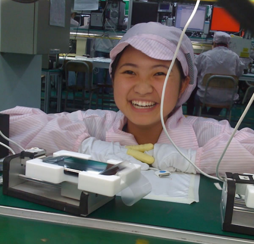
Note: In the early days of the iPhone, the camera function was manually tested. The picture shows the "iPhone Girl" in 2008.
With the development of automation and artificial intelligence, Du Zheng introduced that there are now powerful automation equipment (handlers) and AI detection methods. Mr. Miao Xiaoyong from Tongfu Microelectronics, a packaging company, introduced that it cooperates with Xinshida in WLCSP process (wafer level chip size packaging). Integrating chip-scale packaging (CSP) and wafer-level packaging (WLP) into one, the chip has the characteristics of "short, light and thin", which is in line with the trend of consumer electronics developing toward intelligence and miniaturization.
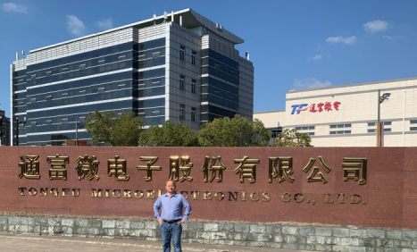
Lao Yao (Wang Yanhui), the founder of Jiwei.com, also tested small equipment in 2007, but later found that he was more talented in the media, but he has always been paying attention to this industry. He said: Many chip design companies will purchase/select test equipment themselves and put them on the test production line.
Coincidentally, Apple does the same thing on its production line.
3、2014 years later, global packaging companies have consolidated, and Chinese companies have used mergers and acquisitions to enter advanced packaging and gain major customers.
Changdian Technology acquired Singapore's STATS ChipPAC, Tongfu Microelectronics acquired AMD's Suzhou and Penzhou packaging and testing plants, Huatian Technology acquired FCI and Unisem companies in the United States, and Jingfang Technology acquired Zhi Ruida and Anteryon companies, etc.
Artificial intelligence has developed greatly, AMD's profits have skyrocketed, Su's mother (Su Zifeng) is smiling from ear to ear, and Tongfu has also followed the rise.
4. Shenzhen Memory drives the rapid development of storage packaging
Huaqiangbei is the earliest professional electronics market in China. PC memory modules are also one of the hottest products in the machine market. This is also where Shenzhen Memory started.
In 2014, with the development of smart phones and mobile Internet (represented by WeChat), the demand for storage has also increased a lot, especially for photos, and the 128G of my mobile phone is not enough. In 2018, the global semiconductor industry reached US$476.7 billion. Among them, memory, as the largest semiconductor category, accounts for nearly 35% of the semiconductor market. That year, mainland China imported approximately US$310 billion in integrated circuits, of which approximately US$100 billion was in storage. Yangtze Memory and Hefei Changxin have their own wafer fabs in mainland China.
The growth potential of mainland brand memory is very good. One area in Shenzhen has gathered many excellent memory brand companies such as Kintek, Creative, Acer, Longsys, Memory, Baiwei, and Jiaho Jinwei (in no particular order). Shenzhen Technology (acquired Kingston's Payton) and Konka have entered the market. These companies have entered the field of chip packaging and module packaging.
Driven by the demand for memory in Shenzhen, companies such as Taiji Semiconductor, Changdian Technology, and Tongfu Microelectronics are also working hard to develop storage packaging and testing.
Here is another story about driving domestic equipment. In 2013, the storage customers of Shenzhen Kaiyi Technology, which provides manufacturing technology solutions for the electronics manufacturing industry, put forward the need for bonded automated inspections. Kaiyi approached suppliers in South Korea and Japan to develop related products, but they were rejected due to high measurement accuracy requirements and software algorithm difficulty. Finally, they cooperated with local manufacturer Shenzhen Octavia. Octavia transplanted its mature SMT experience into the packaging process to achieve online continuous visual inspection. It began to go online in 2015 and was applied to storage, sensor packaging and other products.
5. AIoT and electric vehicles drive a new upsurge in advanced packaging
At the SEMICON CHINA 2021 exhibition, it can be seen that advanced packaging and high-density packaging are developing rapidly.
With the development of the AIoT era, drinking tea (automatically adding water to boil water), smoking (e-cigarettes), opening doors (smart locks), sweeping the floor (robots), and studying at home (laptops) are all equipped with a large number of chips.
Tesla builds factory in Lingang. China has launched new infrastructure and built charging piles, and the electric vehicle and two-wheeled electric vehicle industries have developed greatly, which has brought huge demand for chips. Automotive-grade chips have high requirements for reliability and special requirements for packaging.
The packaging industry is experiencing explosive growth in China, with many companies pouring in. Ningbo took action. The newly established Yongsi Electronics directly positioned itself for advanced packaging and entered the ranks of giants with rapid progress. It is said that it is already ranked very high in the country.
2. Mainland China’s development of packaging and testing: the electronics industry cannot avoid China
Electronic products with mobile phones as the core are China's largest export products, followed by textiles. Do you still remember the joke about 100 million pairs of pants being exchanged for one plane in the early days of reform and opening up?
From a big perspective, the global fight against the epidemic cannot be separated from electronic products; from a small perspective, there are many people who hold their mobile phones when taking a shower!
The supply chain of electronic information technology products is very complex. The numerous parts, complex software and hardware designs and process requirements clearly reflect China’s engineer dividends and manufacturing dividends. Therefore, this is the industry that is most difficult to decouple from China. Even if it is “deglobalized”, it cannot be “de-Sinicized”.
The production process of electronic products is roughly divided into three parts: wafer, packaging, and complete machine manufacturing (SMT surface mounting is the core). The wafer is connected to the packaging test, and the complete machine is connected to the bottom.
Although there are not many people employed in the wafer industry, the technical elements are firmly controlled by the West, and the gap is obvious. There is still a difficult journey to go to completely solve the "stuck neck" problem. It is worth noting that the United States is strengthening the field of wafer manufacturing. TSMC/Samsung/INTEL/GlobalFoundries will vigorously develop wafer manufacturing with the most advanced processes in the United States.
India sells one to two hundred million mobile phones every year, and of course it must develop its manufacturing industry. Mainland China's complete machine manufacturing will inevitably shift part overseas (for example, Apple, Mi OV, etc. already have production capacity in India).
Therefore, from a strategic point of view, it is necessary to strengthen the upstream chip packaging and testing field. Only in this way can China still occupy an important link in the supply chain and ensure that the overall core position of "Made in China" remains unchanged.
Professor Cai Zhikuang from the Nantong Packaging Research Institute of Nanjing University of Posts and Telecommunications said with emotion that the biggest feeling about packaging recently is that "the color changes after smelling it." For example, in a BGA packaging production line, if there is not enough BGA substrate production capacity, they will not dare to take orders rashly. The country should increase investment and move from the "discoloration after hearing the basics" to the "dance after hearing the basics" stage as soon as possible, so that everyone has substrates and every household has production capacity.
This time, as soon as I entered the SEMICON exhibition hall, I bumped into the booths of Shennan Circuit and Tianxin Interconnect. One hand was making packaging substrates, and the other was making advanced packaging.
Jiwei.com’s article tells the reasons behind it: Behind the serious shortage of packaging substrates: upstream materials and equipment have become a bottleneck for production expansion
Lead frame is also an important packaging material, and production capacity is also lacking.
The fact that online design companies are "begging for production capacity" is not groundless.
3. Advanced packaging: combined with wafer and SMT
1, advanced packaging is also high technology
In the early stages of the development of the semiconductor industry, semiconductor packaging has always been regarded as an industry with relatively low technical barriers and relatively intensive labor costs. Packaging is the most difficult industry to make money in the integrated circuit industry chain. It needs to continuously increase investment to earn the marginal increment of every dollar.
As the integration level of chips increases, the technical requirements for semiconductor packaging are getting higher and higher, which makes semiconductor packaging no longer a simple technology. All kinds of advanced packaging and new processes have appeared, which makes me dazzled.
As packaging complexity continues to increase, advanced packaging has become an important source of production increment. In the future, the ratio of the three sections of the chip is expected to be: 3 (design): 4 (wafer): 3 (packaging).
Traditional packaging passively accepts the arrangements of chip design companies. The current trend is that chip design manufacturers increasingly need to conduct collaborative design with packaging manufacturers. In the post-Moore era, chip back-end manufacturing technology will drive the development of chips towards high performance and high density.
At the 2019 Jiwei Semiconductor Summit, Dad Jiang (Jiang Shangyi) believed that the semiconductor industry environment has undergone tremendous changes. This is mainly reflected in the following aspects: First, the progress of Moore's Law has approached the physical limit, and the most advanced silicon processes (such as 7nm, 5nm) can only be used by a very small number of extremely high-demand products (such as mobile phone main chips); second, the progress of packaging and circuit board technology is relatively backward, gradually becoming a bottleneck for system performance; third, the era of chip (design company) diversification is coming, and the market will no longer be in the hands of a few manufacturers. According to different systems and the special needs of each unit, selecting appropriate units and reintegrating them through advanced packaging and circuit board technology will be one of the development trends in the post-Moore era.
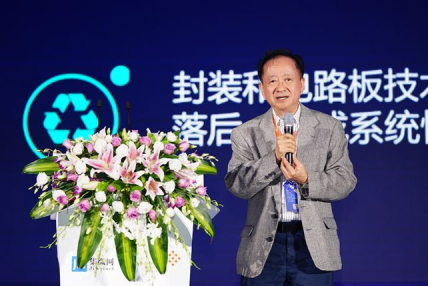
Zheng Li, CEO of Changdian Technology, said: "Semiconductor packaging in today's era is not only the process of sealing the chip into the shell, but also requires dozens of processes for the chip inside, the chip wiring, interconnection interface, and even the need to reorganize the wafer. After that, some chips need to be laid out and interconnected with other chips in the same package, and sometimes it is necessary to Not only that, these chips also need to be connected together at high density to enable their various functional modules to operate organically. Therefore, in the post-Moore’s Law era, packaging is no longer just based on line width and line spacing and integration size, but more about how to improve the performance of the system and how to improve the integration of the entire microsystem.”
2、Combination of packaging and front-end wafer manufacturing
There is shocking news: wafer fabs such as TSMC and SMIC have also entered the wafer-level packaging industry. Originally I thought this was a threat to the packaging industry, but Changdian CEO Zheng Li thinks this is actually a good thing. One development path for advanced packaging is wafer-level packaging (WLP). If wafer-level packaging continues to develop in multi-dimensional directions, such as 2D, 2.5D, and 3D, it will inevitably cooperate with wafer fabs. This is because the wafer fab has the ability to perform TSV (Through Silicon Via) process manufacturing on the wafer. When it comes to silicon transfer boards, the wafer factory can also make Silicon Interposer (silicon interposer), which is a wafer with high-density wiring. The packaging and testing factory has to carry out the RDL (wafer redistribution) process, and then re-integrate the wiring at a high density at the packaging and testing level.
Industry experts commented that there is about a 10% gap in the yield ratio of high-end packaging and testing between Changdian and ASE, which will take time to improve. But it is conceivable that the take-off speed of mainland packaging and testing is faster than that of wafer manufacturing in the previous stage. It is no longer a thing of the past to regard closed beta testing as the backend. Nowadays, there are many intersections between closed beta and the frontend. Challenges are everywhere and require persistence and patience!
3, advanced packaging and SMT surface mount combination
In addition to the integration with wafer manufacturing described above, packaging and testing is also closely integrated with complete machine manufacturing (SMT as the core).
Around 2015, I saw the demo of a multi-chip package for the first time, integrating the required components into a module, reducing the number of packaging and wiring problems, saving space, improving performance, and reducing the cost of the entire machine.
System-in-Package SiP (System in Package) and SMT (Surface Mount) are inseparable. Major equipment manufacturers such as ASM-PT, K&S, etc. originally made SMT placement machines. SiP can reduce issues such as process compatibility, signal mixing, noise interference and electromagnetic interference faced during chip system integration.
Mobile phone RF front-end modules (PAMiD, etc.) largely use SiP or similar processes. Kaiyuan Communications Jia Bin said that the popularization of 5G has brought more and more radio frequency components to mobile phones. If they are packaged separately and then placed on the PCB board for patching, the mobile phone may not fit in them, so it is best to integrate them. The basic processes of radio frequency chips such as SAW, BAW, PA, LNA, and RF Switch are different. SoC solutions cannot be used. Instead, multiple chips can be packaged into modules using system-level packaging and other processes. International big names Skyworks, Qorvo, Avago (acquisition of Broadcom), Qualcomm, etc. do this. I searched online and found that there are many radio frequency processes, such as GaAs, bulk silicon CMOS, SOI insulating substrate silicon, silicon-based MEMS, SiGe silicon germanium, etc.
The camera module and fingerprint recognition module adopt COB (Chip on Board) technology. The chip is not packaged and is directly cut into bare wafers (Dies), deferring bonding and other packaging processes to the module stage.
The common "cow shit chip" also uses the COB process. The bare chip is fixed on the PCB circuit board through Bonding equipment, and then epoxy resin glue is dripped on it. Then other components are attached through the SMT process, and a circuit board is born. This is what the caller identification telephone control board does. The gold wire circles are the many Bonding gold wires surrounding the die.
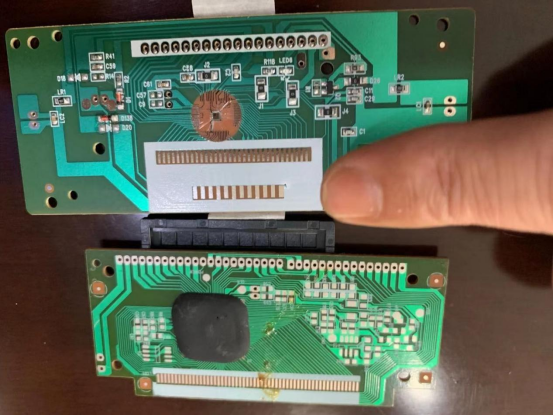
Note: CID phone control panel (photographed by author Dai Hui in Tianxunlong)
4. Advanced packaging: patent disputes
Inevitably, patent battles will also take place in packaging. Mr. Mark, head of Jiweiwang’s IP consulting business, told a classic case of the battle between Chinese and foreign companies over packaging patents, which came from the MEMS microphone industry.
The American company Knowles, which was the first to apply MEMS technology to microphone manufacturing to replace traditional electrets, applied for a basic packaging patent in 2000. Based on this patent, Knowles launched patent infringement lawsuits against American Akustica, Singapore Memstech, American ADI, British Wolfson, South Korean Baoxing, American Amkor, and mainland Goertek in 2006, and even launched a 337 investigation.
Mainland MEMS microphone manufacturer AAC signed a patent licensing agreement with Knowles early on to avoid patent litigation. However, heavy patent licensing fees have also become a reality that mainland companies have to face. In contrast, the industrial chain in Taiwan, China, pays more attention to circumventing Knowles's U.S. patent. Led by the Taiwan Industrial Research Institute, in conjunction with major electroacoustic manufacturers such as Meilu, at least seven patents have been deployed around Knowles' packaging patent to circumvent it. However, it was precisely because of the excessive emphasis on avoiding Knowles' basic patents that Taiwan, China's originally advantageous semiconductor manufacturing advantages were not brought into play in the field of MEMS microphones, missing market opportunities, and ultimately becoming mainland China's AAC and Goertek.
five,seal upPackequipment:"The Rise of the Group"
I have witnessed the rise of telephone and program-controlled switches, mobile communications and mobile phone industry groups, and also brought about the rise of groups in the mainland chip industry. The term "group rise" is most appropriate when used to refer to the packaging and testing equipment industry.
At SEMICONChina 2021, I saw the localization of many categories of packaging and testing equipment. Packaging includes grinding, cutting (DICING), DIE BOND (crystal bonding), WIRE BOND (wire bonding) and other main equipment areas.
The development of domestic equipment will be very helpful in dismantling monopoly, reducing costs, improving performance and improving efficiency.
At the 2020 Packaging Conference held in Tianshui, Hua Tianxiao Shengli said that packaging and testing companies should adhere to the concept of cooperation over competition, actively cultivate the construction of domestic equipment and materials, and gradually complete the test platform.
Using domestic equipment to break the monopoly of Western equipment can effectively reduce costs, which is obvious in packaging.
Xinqi Micro Devices, which has just been listed on the Science and Technology Innovation Board, has filled the gap in domestic maskless lithography equipment. Its direct-write lithography equipment serves the PCB (printed circuit board) and pan-semiconductor (FPD display) fields, and is planning direct-write lithography equipment for wafer-level packaging (WLP). After the listing, the stock price skyrocketed, and the entire semiconductor sector also experienced a rise (hopefully not just a rebound).
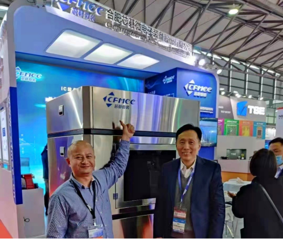
Note: Author Dai Hui and Qu Lujie, chief scientist of Xinqi Micro Devices, at the booth
In terms of die bonding machines, Dongguan Plessin once filled the gap in domestic linear IC-level die bonding machines (DIE BOND).
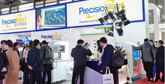
Wang Lin from Beyond Moore Fund contributed a case: Leiming Laser launched laser grooving + laser hidden cutting equipment with performance comparable to that of Western companies, breaking the market monopoly.
6. Test Equipment: “The Rise of Groups”
The testing equipment mainly includes the sorting machine Handler for chip-level testing, the probe station Probe for wafer-level testing, and the automatic testing machine ATE.
There are great opportunities for localization of testing equipment. New processes bring customization needs, and domestic equipment may be used in one step to achieve higher efficiency and better performance.
Shenzhen Silicon Electric is a manufacturer of probe stations and sorting machines.
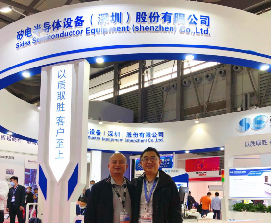
Note: Author Dai Hui and Professor Hu Hong of Harbin Institute of Technology at the silicone booth
Zhang Yue, CEO of Yuexin Technology, introduced me to the main product Memory memory testing equipment, which has done a lot of work on high efficiency, consistency, and stability.
Accelerate Technology launches high-performance ATE automatic testing machine, combined with artificial intelligence.
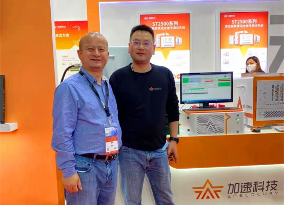
Note: Author Dai Hui and Acceleration Technology CEO Wu Gang at the booth
Shaoxing Hongbang displayed a variety of power device testing machines and sorting machines. I "rolled up my sleeves" and tried them out.
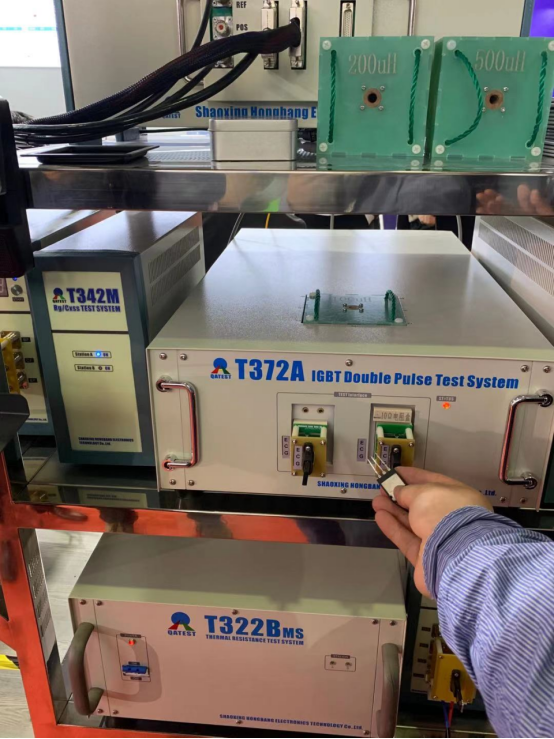
Note: Discrete device testing machine exhibited by Shaoxing Hongbang
Nanjing Hongtai Semiconductor displayed a series of semiconductor ATE automated testing products. In 2019, it wholly acquired Japan's Azurtest Co., Ltd. (Azurtest), which is famous for analog testing technology.
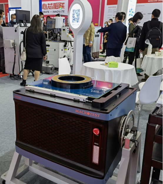
Note: Hongtai Semiconductor exhibits mixed-signal test machine MS8000
Related service companies are also developing. Shanghai Jifeng Electronics has services such as material analysis, failure analysis and reliability certification.
seven,Packaging materials:steady development
In the field of materials, mainland China is also catching up, such as substrates and lead frames that have recently "discussed base color change".
The electronics industry uses a large amount of precious metal gold, mainly in wire bonding of packages. The industry continues to promote the use of copper (or even aluminum) to replace gold in more and more scenarios, and mainland companies have also done a lot of work.
Shenzhen's chip manufacturing industry is slower than some domestic cities, so it plans to overtake in corners. Starting in 2020, Shenzhen will promote the development of a new generation of information and communication technology. Bi Yalei, secretary-general of the Shenzhen Robot Association, said that on December 30, 2020, the Advanced Academy of Sciences of the Chinese Academy of Sciences established the Shenzhen International Innovation Institute of Advanced Electronic Materials (hereinafter referred to as the "Electronic Materials Institute") in Bao'an, focusing on high-end advanced electronic packaging materials and aiming to promote the localization of high-end electronic materials to "break through."
8. True “core” hero: Don’t forget the original “core” and accumulate thousands of miles of silicon
Mr. Ding Wenwu, the head of the National Integrated Circuit Fund, posted a song "True "Chip" Heroes", singing the "core" sentiments of many chip people: use our "cores" to realize China's "core dream" together; let our "cores" be like the stars and the sea, making the world interconnected and interactive.
Disclaimer: This article is reproduced from "Dai Hui Steve", which supports the protection of intellectual property rights. Please indicate the original source and author when reprinting. If there is any infringement, please contact us to delete it.
Related Recommendations
Exclusive Interview with Li Gang of Yunfan Ruida: The Precision of Millimeter-Wave Radar Products and the Warmth of Humanity
2026-07-22
2518
RF Passion, Craftsman’s Journey: Over 30 Years of Steadfast Dedication — Interview with Kinghelm Chief Engineer Mr. Qin hongxiang
2026-06-26
2688





 粤公网安备44030002007346号