10,000伏!国产氮化镓再创全球纪录
2022-03-17 301
最近的,Suzhou Jingzhan SemiconductorThe official website announced,其最新研发的氮化镓器件创造了新的纪录 - 击穿电压超过10千伏,"This is by far the highest value in the world."

More importantly, the GaN epitaxial structure of the device is based on a sapphire substrate, so the preparation cost is higher than that of SiC价格便宜2-3倍。景占认为,这一突破将有助于氮化镓突破瓶颈。Electric vehicles, power grids and rail transitand other high-voltage application fields, with broad potential.
Interruption: To join the third-generation semiconductor tycoon group, please add WeChat: hangjiashuo666.

Innovative extension architecture

创造世界最高纪录
According to Jingzhan, they worked withVirginia Tech Power Electronics Technology Center(CPES) cooperated to tackle key problems and prepared a GaN SBD, successfully achieving an ultra-high breakdown voltage of more than 10kV, which is the highest record of breakdown voltage of GaN power devices so far.
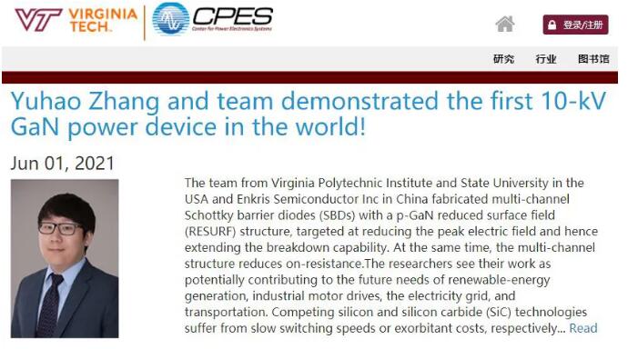
On June 1, CPES also announced this matter.
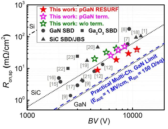
After measurement, the breakdown voltage of one of the gallium nitride devices prepared by Jingzhan is approximately11kV电容-电压测量(反向偏置电压高达 3kV)表明,电容能量损耗仅为1.6μJ/mm
Moreover, while achieving an ultra-high breakdown voltage of 10kV, the device has a Baliga figure of merit of up to2.8GW?厘米2, the on-resistance is as low as39mΩ·cm2远低于10kVVoltage-resistant SiC SBD.
There are two key technologies for this technological breakthrough, including Suzhou Jingzhan’s newMulti-channel AlGaN/GaN heterostructure epitaxial wafer,也pGaN表面场抑制技术(表面处理)
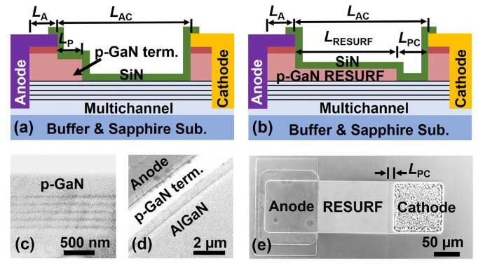
Among them, Jingzhan’s gallium nitride epitaxial material structure includes: 20nm p+GaN/350nm p-GaN cap layer, and 5 channels of 23nm Al0.25Ga0.75N/100nmGaN intrinsic layer.
Figure 1: Multi-channel AlGaN/GaN SBD device structure diagram

基于蓝宝石

比碳化硅便宜3倍

It is understood that this epitaxial structure was created by Jingzhan’s team through MOCVD method on a 4-inch蓝宝石衬底无需二次外延即可实现单次连续外延。由于采用了廉价的蓝宝石衬底和水平器件结构,器件制备成本远低于其他方法。碳化硅二极管
研究团队指出,与4英寸碳化硅(SiC)相比,4英寸蓝宝石衬底氮化镓(GaN)晶圆的成本有所降低。About 2-3 times此外,景展器件的芯片尺寸更小,因此器件的材料成本远低于同级别的SiC SBD,横向GaN器件的加工成本也低于SiC。
In addition, the team estimated that 10kV, 0.3ARESURF device开关质量系数为15.7nCV, while 3.3kV, 0.3ASIC SBDHPMC胶囊30.8nCV

Figure 2: Jing ZhanSBD与其他氮化镓SiC, gallium oxideSBD导通电阻和BVComparison of benchmarks (the dotted line is the theoretical limit).


免责声明:本文转载自《第三代半导体趋势》。本文仅代表作者个人观点,不代表赛科微电子及业界立场。转载仅供参考,以支持知识产权保护。转载请注明原文出处及作者。如有任何侵权行为,请联系我们删除。


whatsapp

WhatsApp

Whatsapp:+8618073002950