News
News
10,000 volts! ! Domestic GaN sets another global record
2022-03-17 300
recent,Suzhou Jingzhan SemiconductorThe official website announced,Its latest developed GaN device has set a new record——Breakdown voltageexceeds 10kV,"This is by far the highest value in the world."

More importantly, the GaN epitaxial structure of the device is based on a sapphire substrate, so the preparation cost is higher than that of SiC2-3 times cheaper.Jingzhan believes that this breakthrough will help gallium nitride break intoElectric vehicles, power grids and rail transitand other high-voltage application fields, with broad potential.
Interruption: To join the third-generation semiconductor tycoon group, please add WeChat: hangjiashuo666.

Innovative extension architecture

Set the world's highest record

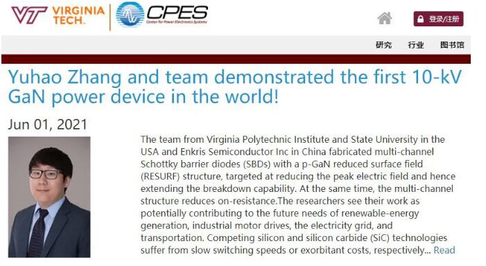
According to Jingzhan, they worked withVirginia Tech Power Electronics Technology Center(CPES) cooperated to tackle key problems and prepared a GaN SBD, successfully achieving an ultra-high breakdown voltage of more than 10kV, which is the highest record of breakdown voltage of GaN power devices so far.
On June 1, CPES also announced this matter.
After measurement, the breakdown voltage of one of the gallium nitride devices prepared by Jingzhan is approximately11kV. Capacitance-voltage measurements up to 3kV reverse biased show that the capacitive energy loss is only1.6μJ/mm
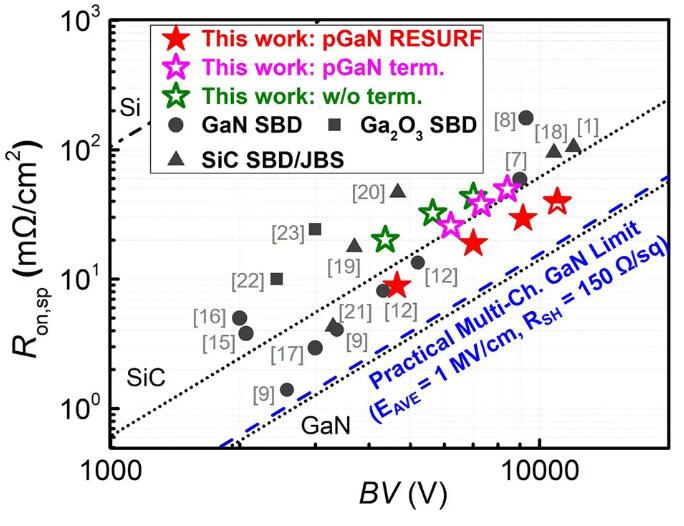
Moreover, while achieving an ultra-high breakdown voltage of 10kV, the device has a Baliga figure of merit of up to2.8GW?cm2, the on-resistance is as low as39mΩ?cm2, much lower than10kVVoltage-resistant SiC SBD.
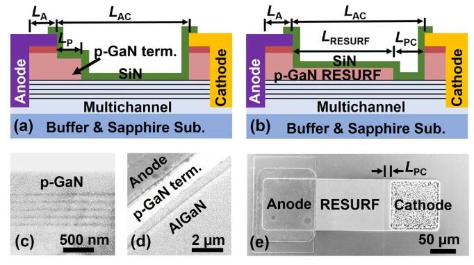
There are two key technologies for this technological breakthrough, including Suzhou Jingzhan’s newMulti-channel AlGaN/GaN heterostructure epitaxial wafer,as well aspGaN surface field reduction technology(RESURF)。
Among them, Jingzhan’s gallium nitride epitaxial material structure includes: 20nm p+GaN/350nm p-GaN cap layer, and 5 channels of 23nm Al0.25Ga0.75N/100nmGaN intrinsic layer.
Figure 1: Multi-channel AlGaN/GaN SBD device structure diagram

Based on sapphire

3 times cheaper than SiC

It is understood that this epitaxial structure was created by Jingzhan’s team through MOCVD method on a 4-inchSapphire substrateA single continuous epitaxy is achieved without the need for secondary epitaxy. Due to the use of cheap sapphire substrate and horizontal device structure, the device preparation cost is much lower thanSiC diode
The team noted the cost reduction of 4-inch GaN on sapphire wafers compared to 4-inch SiCAbout 2-3 times. In addition, the chip size of Jingzhan devices is smaller, so the material cost of the device is much lower than that of SiC SBD of the same level, and the processing cost of lateral GaN devices is also lower than SiC.
In addition, the team estimated that 10kV, 0.3ARESURF deviceThe switching quality factor is15.7nCV, while 3.3kV, 0.3ASIC SBDfor30.8nCV

Figure 2: Jing ZhanSBDwith otherGaNSiC, gallium oxideSBDon-resistance andBVComparison of benchmarks (the dotted line is the theoretical limit).


Disclaimer: This article is reproduced from "Third Generation Semiconductor Trend". This article only represents the author's personal views and does not represent the views of Sacco Micro and the industry. It is only for reprinting and sharing to support the protection of intellectual property rights. Please indicate the original source and author for reprinting. If there is any infringement, please contact us to delete it.


whatsapp

Service Hotline

tel: +86 755 83044319

WhatsApp

Whatsapp:+8618073002950