
























सेवा हॉटलाइन
समाचार

समाचार
कोई माइक्रोट्यूब्यूल दोष नहीं! 6-इंच SiC एक और सामान्य विशेषता जोड़ता है।
2022-03-17
827
Recently, domestic SiC substrates have made new progress——टोंगगुआंग क्रिस्टल ने माइक्रो पाइप दोषों के बिना 6 इंच का SiC सिंगल क्रिस्टल सफलतापूर्वक तैयार किया।"More suitable for making high-voltage and ultra-high-voltage power devices."
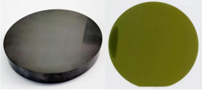
According to reports, the same optical crystal adoptsImproved PVT growth design plan, its 6-inch SiC wafer does not have any stress spots, the base plane of the lattice is less curved, the average half-peak width of its (004) diffraction index is as low as 19 arc seconds, and the resistivity distribution is uniform.
The results were published in the April 2021 issue of "Acta Ceramics" and the submission time was July 2020.
Innovative growth process
Solving the problem of microtubule defects
लगभग 30 वर्षों की कड़ी मेहनत के बाद, उद्योग ने माइक्रो पाइप दोषों के बिना 2-4 इंच 4H-SiC एकल क्रिस्टल सामग्री को परिपक्व रूप से तैयार करने में सफलता प्राप्त कर ली है। हालाँकि,6 इंच के 4H-SiC सिंगल क्रिस्टल में अभी भी कुछ कठिनाइयाँ हैं।Tongguang Crystal believes that to prepare 6-inch SiC single crystals without micropipe defects, the generation of polytypes should be avoided, and their method isभौतिक वाष्प परिवहन (पीवीटी) विधि में संशोधन।According to reports, under conventional growth assembly conditions, the direction of growth component flow is partly in the same direction as the growth step flow direction, and part of it is opposite to the step flow direction. The improvement plan of the same optical crystalAdopts drainage assembly or asymmetric temperature field design, during the growth process, the direction of the growth component flow is almost always opposite to the direction of the step flow.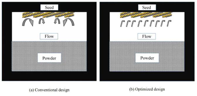 चित्र 1: दो पीवीटी विधियों का योजनाबद्ध आरेख This improved process has unique advantages——The component atoms on the single crystal growth surface can quickly reach the kink position of the growth step, ensuring the orderly advancement of the atomic steps, thereby completely replicating the crystal structure of the single crystal. In addition, the orderly advancement of steps will not cause the aggregation of steps, and will not produce wide steps, thus avoiding the two-dimensional polytype nucleation phenomenon caused by wide steps. therefore,इस उन्नत प्रक्रिया से 6 इंच के एन-टाइप SiC सिंगल क्रिस्टल की स्थिरता में काफी सुधार हुआ है।
उत्कृष्ट प्रदर्शन
Meet power device needs
According to the paper, the Raman spectrum detection scan results of the substrate wafer showed that,The entire 6-inch wafer is a single 4H-SiC crystal form.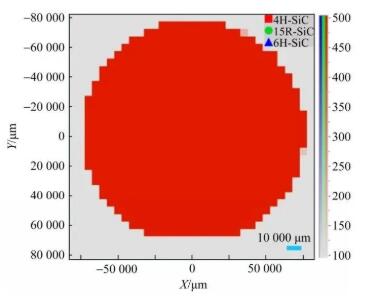 चित्र 2: 6-इंच SiC रमन स्पेक्ट्रम स्कैनThrough the polarization stress meter, it was found that after improving the growth process conditions,चिप मेंNo stress spots,This shows that the crystal quality of the grown SiC single crystal is better.
 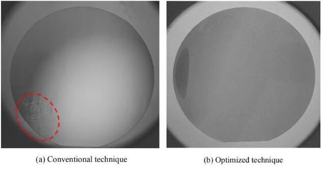 चित्र 3: दो प्रक्रियाओं का उपयोग करके वेफर्स के ध्रुवीकरण तनाव वितरण की तुलनाHigh-resolution XRD rocking curve mode test results show that the orientation difference of the entire wafer is within 0.04°, and the radius of curvature in the X-axis direction is ≥132 m,इससे पता चलता है कि इसकी जाली का आधार तल कम घुमावदार है और इसमें स्टैकिंग दोष कम हैं।इसके अतिरिक्त, इसके परीक्षण रॉकिंग वक्रों की अधिकांश अर्ध-शिखर चौड़ाई 30 आर्क सेकंड से कम है, और औसत अर्ध-शिखर चौड़ाई 19 आर्क सेकंड है, जो दर्शाता है कि इसकी क्रिस्टल गुणवत्ता बहुत उच्च है।इसके अंदर बहुत ज्यादा सूक्ष्म खामियां नहीं हैं।
 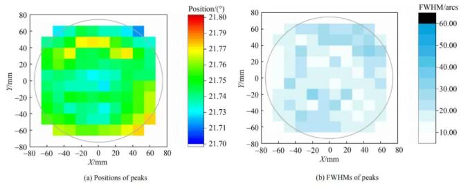 चित्र 4: 6 इंच के SiC एकल क्रिस्टल के (004) क्रिस्टल तल का उच्च-रिज़ॉल्यूशन XRD रॉकिंग वक्र स्कैन।साथ ही, एड़ी करंट विधि परीक्षण के परिणामों से पता चलता है कि इसकी प्रतिरोधकता का मान 16.8-22.2 mΩcm के बीच है। प्रतिरोधकता वितरण एकसमान है, और सांख्यिकीय विक्षेपण गुणांक 3.5% है। औसत प्रतिरोधकता मान 20.5 mΩcm है।यह विद्युत उपकरणों की उत्पादन आवश्यकताओं को अच्छी तरह से पूरा कर सकता है।
 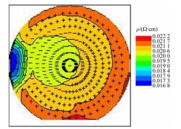 Figure 5: Resistivity distribution diagram of 6-inch n-type SiC single crystal wafer
अस्वीकरण: यह लेख "थर्ड जेनरेशन सेमीकंडक्टर ट्रेंड" से लिया गया है। यह लेख केवल लेखक के निजी विचारों को दर्शाता है और सैको माइक्रो या उद्योग जगत के विचारों का प्रतिनिधित्व नहीं करता है। इसका पुनर्मुद्रण और साझाकरण केवल बौद्धिक संपदा अधिकारों के संरक्षण के लिए किया जा सकता है। पुनर्मुद्रण के लिए कृपया मूल स्रोत और लेखक का उल्लेख करें। यदि कोई उल्लंघन होता है, तो कृपया इसे हटाने के लिए हमसे संपर्क करें।
कंपनी का फ़ोन नंबर: +86-0755-83044319
फैक्स: +86-0755-83975897
ईमेल: 1615456225@qq.com
QQ: 3518641314 मैनेजर ली
QQ: 332496225 प्रबंधक किउ
पता: कमरा नंबर 809, बिल्डिंग सी, झांताओ टेक्नोलॉजी बिल्डिंग, 1079 मिंझी एवेन्यू, लोंगहुआ न्यू डिस्ट्रिक्ट, शेन्ज़ेन
संबंधित अनुशंसाएँ
युनफान रुइडा के ली गैंग के साथ विशेष साक्षात्कार: मिलीमीटर-वेव रडार उत्पादों की सटीकता और मानवता की गर्मजोशी
2026-07-22
2545
आरएफ के प्रति जुनून, एक कुशल कारीगर का सफर: 30 वर्षों से अधिक का अटूट समर्पण — किंगहेल्म के मुख्य अभियंता श्री किन होंगशियांग के साथ साक्षात्कार
2026-06-26
2714





 粤公网安备44030002007346号