
























Service Hotline
News

News
No microtubule defects! 6-inch SiC adds another general
2022-03-17
826
Recently, domestic SiC substrates have made new progress——Tongguang Crystal successfully prepared a 6-inch SiC single crystal without micropipe defects."More suitable for making high-voltage and ultra-high-voltage power devices."
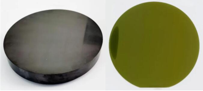
According to reports, the same optical crystal adoptsImproved PVT growth design plan, its 6-inch SiC wafer does not have any stress spots, the base plane of the lattice is less curved, the average half-peak width of its (004) diffraction index is as low as 19 arc seconds, and the resistivity distribution is uniform.
The results were published in the April 2021 issue of "Acta Ceramics" and the submission time was July 2020.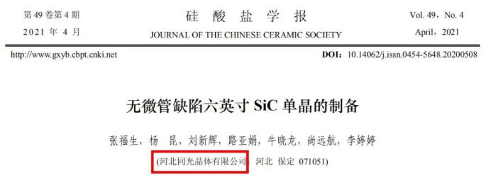
Innovative growth process
Solving the problem of microtubule defects
After nearly 30 years of hard work, the industry has been able to maturely prepare 2-4-inch 4H-SiC single crystal materials without micropipe defects. However,There are still certain difficulties in 6-inch 4H-SiC single crystal.Tongguang Crystal believes that to prepare 6-inch SiC single crystals without micropipe defects, the generation of polytypes should be avoided, and their method isModification of the physical vapor transport (PVT) method.According to reports, under conventional growth assembly conditions, the direction of growth component flow is partly in the same direction as the growth step flow direction, and part of it is opposite to the step flow direction. The improvement plan of the same optical crystalAdopts drainage assembly or asymmetric temperature field design, during the growth process, the direction of the growth component flow is almost always opposite to the direction of the step flow.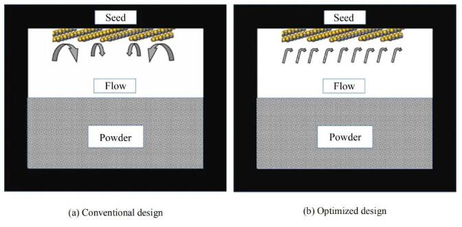 Figure 1: Schematic diagram of two PVT methods This improved process has unique advantages——The component atoms on the single crystal growth surface can quickly reach the kink position of the growth step, ensuring the orderly advancement of the atomic steps, thereby completely replicating the crystal structure of the single crystal. In addition, the orderly advancement of steps will not cause the aggregation of steps, and will not produce wide steps, thus avoiding the two-dimensional polytype nucleation phenomenon caused by wide steps. therefore,The improved process has greatly improved the stability of the 6-inch n-type SiC single crystal.
Excellent performance
Meet power device needs
According to the paper, the Raman spectrum detection scan results of the substrate wafer showed that,The entire 6-inch wafer is a single 4H-SiC crystal form.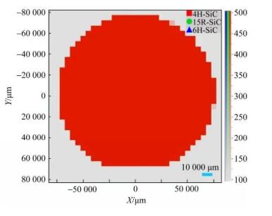 Figure 2: 6-inch SiC Raman spectrum scanThrough the polarization stress meter, it was found that after improving the growth process conditions,in chipNo stress spots,This shows that the crystal quality of the grown SiC single crystal is better.
 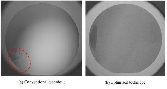 Figure 3: Comparison of polarization stress distribution of wafers using two processesHigh-resolution XRD rocking curve mode test results show that the orientation difference of the entire wafer is within 0.04°, and the radius of curvature in the X-axis direction is ≥132 m,This shows that the base plane of its lattice is less curved and there are fewer stacking faults.In addition, most of the half-peak widths of its test rocking curves are below 30 arc seconds, and the average half-peak width is 19 arc seconds, which indicates that its crystal quality is very high.There aren't a lot of microscopic flaws inside.
 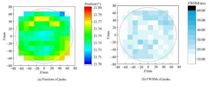 Figure 4: High-resolution XRD rocking curve scan of the (004) crystal plane of a 6-inch SiC single crystal.At the same time, the eddy current method test results show that its resistivity value is between 16.8-22.2 m?cm. The resistivity distribution is uniform, and the statistical dispersion coefficient is 3.5%. The average resistivity value is 20.5 m?cm,It can well meet the production requirements of power devices.
 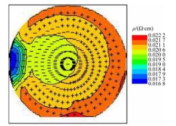 Figure 5: Resistivity distribution diagram of 6-inch n-type SiC single crystal wafer
Disclaimer: This article is reproduced from "Third Generation Semiconductor Trend". This article only represents the author's personal views and does not represent the views of Sacco Micro and the industry. It is only for reprinting and sharing to support the protection of intellectual property rights. Please indicate the original source and author for reprinting. If there is any infringement, please contact us to delete it.
Company phone number: +86-0755-83044319
Fax/FAX: +86-0755-83975897
Email: 1615456225@qq.com
QQ: 3518641314 Manager Li
QQ: 332496225 Manager Qiu
Address: Room 809, Building C, Zhantao Technology Building, No. 1079 Minzhi Avenue, Longhua New District, Shenzhen
Related Recommendations
Exclusive Interview with Li Gang of Yunfan Ruida: The Precision of Millimeter-Wave Radar Products and the Warmth of Humanity
2026-07-22
2544
RF Passion, Craftsman’s Journey: Over 30 Years of Steadfast Dedication — Interview with Kinghelm Chief Engineer Mr. Qin hongxiang
2026-06-26
2713





 粤公网安备44030002007346号