
























Hotline
Actualités

Actualités
Une percée technologique dans l'épitaxie du carbure de silicium pourrait changer la structure industrielle
2022-03-17
921
my country's silicon carbide industry may usher in epic benefits
Depuis le début de l'année 2021, dans le domaine de l'épitaxie du carbure de silicium, les entreprises nationales et étrangères ont annoncé les bonnes nouvelles les unes après les autres.
Le 1er mars 2021, la société japonaise Toyota Tsusho Co., Ltd. a annoncé officiellement le développement réussi d'une technologie de nanocontrôle de surface, appelée Dynamic AGE-ing. Cette technologie permet de réduire la dislocation du plan de base (BPD) des substrats SiC, quelle que soit leur taille ou leur provenance, à moins de 1.
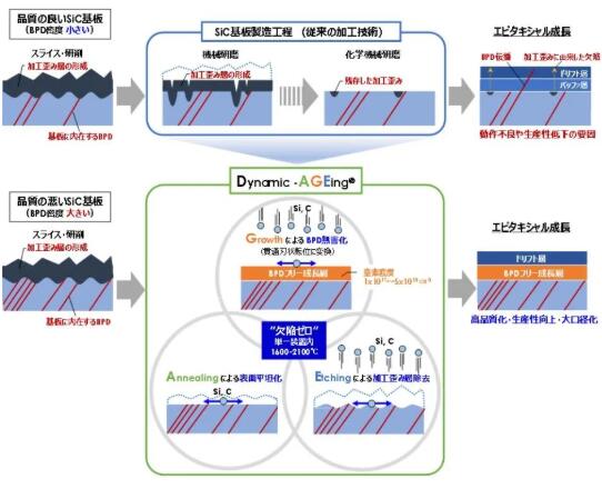 Figure 1 Technologie de vieillissement dynamique Toyota
 Par coïncidence, le 3 mars 2021, Hantian Tiancheng Electronic Technology (Xiamen) Co., Ltd. a annoncé avoir percé le processus de fabrication clé de l'épitaxie par tranchée profonde à superjonction de carbure de silicium.
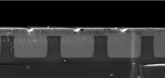 image2 Procédés de fabrication clés pour l'épitaxie en tranchée profonde à superjonction de carbure de silicium
 Silicon carbide epitaxy is an important part of the silicon carbide industry chain. Now that the development of silicon carbide epitaxy technology has entered the fast lane, what impact will it have on the entire silicon carbide epitaxy ecosystem? Please allow me to come one by one.
It may change the international silicon carbide epitaxy industry pattern
The silicon carbide industry chain is mainly divided into several important links such as wafer preparation, epitaxial growth, device manufacturing, module packaging and testing, and system application. Among them, epitaxial growth is an important link between the past and the next and plays a very critical role.
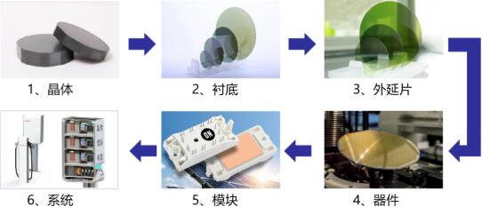 Figure 3 Silicon carbide industry chainBecause existing devices are basically implemented on the epitaxial layer, the quality requirements for the epitaxial layer are very high. And as the voltage resistance continues to improve, the required thickness of the epitaxial layer becomes thicker. Generally, when the voltage is around 600V, the required epitaxial layer thickness is about 6 microns; when the voltage is between 1200-1700V, the required epitaxial layer thickness reaches 10-15 microns. If the voltage reaches more than 10,000 volts, an epitaxial layer thickness of more than 100 microns may be required. As the thickness of the epitaxial layer continues to increase, it becomes increasingly difficult to control thickness and resistivity uniformity and defect density.
 Currently, the mainstream technologies for silicon carbide epitaxy include oblique step flow technology and TCS technology, etc.
The so-called bevel cutting step flow technology is to cut an off angle of about 8° when cutting the silicon carbide substrate. The surface of the substrate cut out in this way produces a high step flow density, making it easy to achieve wafer-level silicon carbide epitaxy. At present, the oblique step flow technology is relatively mature. However, this technology also has two flaws: first, this technology cannot block basal plane dislocations; second, this technology will cause waste of substrate material.
Afin de surmonter les limitations de la technologie de dépôt par étapes, l'ajout de sources de silicium chlorées dans la chambre de réaction a permis, grâce à des améliorations continues, de développer des technologies telles que la TCS (Trical Coefficient de Tris). Aujourd'hui, la technologie d'épitaxie du carbure de silicium est fortement intégrée aux équipements dédiés. En 2014, la TCS et d'autres technologies ont été commercialisées pour la première fois par la société italienne LPE. En 2017, AIXTRON a modernisé les équipements et intégré cette technologie à ses installations commerciales.
Currently, silicon carbide epitaxial equipment is mainly monopolized by Italy's LPE Company, Germany's AIXTRON Company and Japan's Nuflare Company.
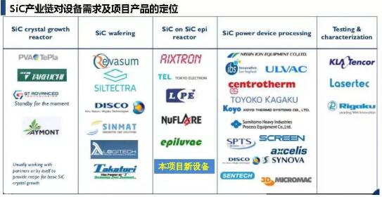 image4 Global silicon carbide industry landscape
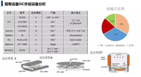
Figure 5 Analyse des équipements d'épitaxie au carbure de silicium existants
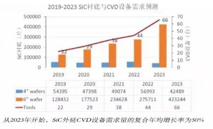 Figure 6 Market prospects of silicon carbide epitaxy equipment
 Avec l'essor de la technologie émergente d'épitaxie du carbure de silicium, cette industrie multimilliardaire pourrait connaître une nouvelle vague de bouleversements.
Cela pourrait contribuer à la maturation de l'industrie des matériaux de substrat en carbure de silicium dans mon pays.
Silicon carbide is a typical representative of the third generation of semiconductor materials. According to different uses, it can be divided into jewelry-grade silicon carbide materials, N-type silicon carbide materials for power electronic devices and semi-insulating silicon carbide materials for power radio frequency devices. Although the market for jewelry-grade silicon carbide materials and semi-insulating silicon carbide materials has grown rapidly in recent years, N-type silicon carbide materials will be the absolute protagonist of the future market.
Compared with jewelry-grade silicon carbide and semi-insulating silicon carbide materials, N-type silicon carbide materials have higher requirements for crystal quality. In this field, there is still a certain gap between my country's silicon carbide substrate companies and CREE's international first-class companies.
If technologies such as Dynamic AGE-ing developed by Toyota can be applied on a large scale in my country, the entry barrier for N-type silicon carbide substrate materials will undoubtedly be greatly reduced. According to statistics from the Semiconductor Materials Branch of the China Electronic Materials Industry Association, we have launched more than 30 silicon carbide substrate material projects, with investments exceeding 30 billion yuan. However, due to technical reasons such as defects, the production capacity of N-type silicon carbide substrates has been delayed. If silicon carbide epitaxial technology achieves a key breakthrough, this will be tantamount to opening the floodgates for my country's silicon carbide substrate material companies.
It may promote my country's silicon carbide device industry
Bien que mon pays ait investi dans plus de 30 projets de substrats en carbure de silicium, les plaquettes de carbure de silicium de type N de 6 pouces, qui représentent la plus forte demande du marché, restent fortement dépendantes des importations. Le coût des substrats et de l'épitaxie en carbure de silicium représente actuellement plus de 50 % du coût total des modules en carbure de silicium. Si ce problème n'est pas résolu, il sera difficile pour l'industrie chinoise du carbure de silicium d'être véritablement compétitive face aux États-Unis.
Market research unit Yole pointed out that the development of the silicon carbide power electronics industry has high potential, and manufacturers including ROHM, Bombardier, Cree, SDK, STMicroelectronics, Infineon Technologies, Littelfuse, Ascatron and other manufacturers have invested heavily. Yole predicts that the SiC power semiconductor market size is expected to reach US$1.4 billion by 2023, with a compound growth rate (CAGR) of 28% from 2016 to 2023, and the CAGR will further increase to 40% from 2020 to 2022.
All in all, the future has broad prospects, but colleagues in the domestic silicon carbide industry should still be encouraged to move forward.
Disclaimer: This article is reprinted from "GaN World". This article only represents the author's personal views and does not represent the views of Sacco Micro and the industry. It is only reprinted and shared to support the protection of intellectual property rights. Please indicate the original source and author when reprinting. If there is any infringement, please contact us to delete it.
Numéro de téléphone de l'entreprise : +86-0755-83044319
Fax/FAX : +86-0755-83975897
Courriel : 1615456225@qq.com
QQ : 3518641314 Gestionnaire Li
QQ : 332496225 Gestionnaire Qiu
Adresse : Salle 809, Bâtiment C, Immeuble technologique Zhantao, n° 1079 avenue Minzhi, Nouveau district de Longhua, Shenzhen
Recommandations connexes
Entretien exclusif avec Li Gang de Yunfan Ruida : La précision des produits radar à ondes millimétriques et la chaleur humaine
2026-07-22
2526
Passion RF, parcours d'artisan : plus de 30 ans d'engagement indéfectible — Entretien avec M. Qin Hongxiang, ingénieur en chef chez Kinghelm
2026-06-26
2690





 粤公网安备44030002007346号