
























Service Hotline
News

News
Silicon carbide epitaxy technology breakthrough may change the industrial structure
2022-03-17
922
my country's silicon carbide industry may usher in epic benefits
Since entering 2021, in the field of silicon carbide epitaxy, domestic and foreign companies have made good news one after another.
On March 1, 2021, Toyota Tsusho Co., Ltd. of Japan officially announced the successful development of a surface nanocontrol technology-Dynamic AGE-ing. This technology can reduce the BPD (base plane dislocation) of SiC substrates of any size and supplier to less than 1.
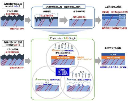 Figure 1 Toyota Dynamic AGE-ing technology
 Coincidentally, on March 3, 2021, Hantian Tiancheng Electronic Technology (Xiamen) Co., Ltd. announced that it had broken through the key manufacturing process of silicon carbide superjunction deep trench epitaxy.
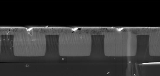 picture2 Key manufacturing processes for silicon carbide superjunction deep trench epitaxy
 Silicon carbide epitaxy is an important part of the silicon carbide industry chain. Now that the development of silicon carbide epitaxy technology has entered the fast lane, what impact will it have on the entire silicon carbide epitaxy ecosystem? Please allow me to come one by one.
It may change the international silicon carbide epitaxy industry pattern
The silicon carbide industry chain is mainly divided into several important links such as wafer preparation, epitaxial growth, device manufacturing, module packaging and testing, and system application. Among them, epitaxial growth is an important link between the past and the next and plays a very critical role.
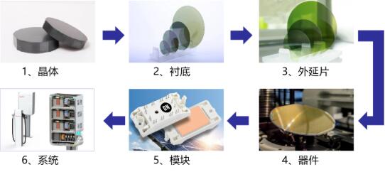 Figure 3 Silicon carbide industry chainBecause existing devices are basically implemented on the epitaxial layer, the quality requirements for the epitaxial layer are very high. And as the voltage resistance continues to improve, the required thickness of the epitaxial layer becomes thicker. Generally, when the voltage is around 600V, the required epitaxial layer thickness is about 6 microns; when the voltage is between 1200-1700V, the required epitaxial layer thickness reaches 10-15 microns. If the voltage reaches more than 10,000 volts, an epitaxial layer thickness of more than 100 microns may be required. As the thickness of the epitaxial layer continues to increase, it becomes increasingly difficult to control thickness and resistivity uniformity and defect density.
 Currently, the mainstream technologies for silicon carbide epitaxy include oblique step flow technology and TCS technology, etc.
The so-called bevel cutting step flow technology is to cut an off angle of about 8° when cutting the silicon carbide substrate. The surface of the substrate cut out in this way produces a high step flow density, making it easy to achieve wafer-level silicon carbide epitaxy. At present, the oblique step flow technology is relatively mature. However, this technology also has two flaws: first, this technology cannot block basal plane dislocations; second, this technology will cause waste of substrate material.
In order to break through the limitations of step flow technology, people tried to add silicon sources containing chlorine elements into the reaction chamber, and finally developed technologies such as TCS through continuous improvement. At present, silicon carbide epitaxy technology has been highly integrated with silicon carbide epitaxy equipment. In 2014, TCS and other technologies were first commercialized by the Italian LPE company. In 2017, AIXTRON upgraded the equipment and transplanted this technology into commercial equipment.
Currently, silicon carbide epitaxial equipment is mainly monopolized by Italy's LPE Company, Germany's AIXTRON Company and Japan's Nuflare Company.
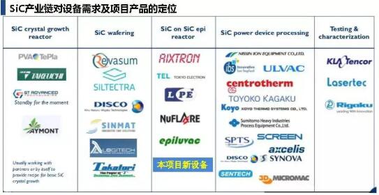 picture4 Global silicon carbide industry landscape
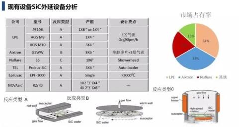
Figure 5 Analysis of existing silicon carbide epitaxy equipment
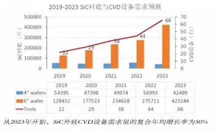 Figure 6 Market prospects of silicon carbide epitaxy equipment
 With the rise of emerging silicon carbide epitaxy technology, this multi-billion industry may usher in a new round of reshuffle.
It may mature my country's silicon carbide substrate material industry
Silicon carbide is a typical representative of the third generation of semiconductor materials. According to different uses, it can be divided into jewelry-grade silicon carbide materials, N-type silicon carbide materials for power electronic devices and semi-insulating silicon carbide materials for power radio frequency devices. Although the market for jewelry-grade silicon carbide materials and semi-insulating silicon carbide materials has grown rapidly in recent years, N-type silicon carbide materials will be the absolute protagonist of the future market.
Compared with jewelry-grade silicon carbide and semi-insulating silicon carbide materials, N-type silicon carbide materials have higher requirements for crystal quality. In this field, there is still a certain gap between my country's silicon carbide substrate companies and CREE's international first-class companies.
If technologies such as Dynamic AGE-ing developed by Toyota can be applied on a large scale in my country, the entry barrier for N-type silicon carbide substrate materials will undoubtedly be greatly reduced. According to statistics from the Semiconductor Materials Branch of the China Electronic Materials Industry Association, we have launched more than 30 silicon carbide substrate material projects, with investments exceeding 30 billion yuan. However, due to technical reasons such as defects, the production capacity of N-type silicon carbide substrates has been delayed. If silicon carbide epitaxial technology achieves a key breakthrough, this will be tantamount to opening the floodgates for my country's silicon carbide substrate material companies.
It may promote my country's silicon carbide device industry
Although my country has invested in more than 30 silicon carbide substrate projects, the 6-inch N-type silicon carbide wafers with the largest market demand still rely heavily on imports. The cost of silicon carbide substrate and epitaxy currently accounts for more than 50% of the total cost of silicon carbide modules. If this problem is not solved, it will be difficult for my country's silicon carbide industry to be very competitive compared with the United States.
Market research unit Yole pointed out that the development of the silicon carbide power electronics industry has high potential, and manufacturers including ROHM, Bombardier, Cree, SDK, STMicroelectronics, Infineon Technologies, Littelfuse, Ascatron and other manufacturers have invested heavily. Yole predicts that the SiC power semiconductor market size is expected to reach US$1.4 billion by 2023, with a compound growth rate (CAGR) of 28% from 2016 to 2023, and the CAGR will further increase to 40% from 2020 to 2022.
All in all, the future has broad prospects, but colleagues in the domestic silicon carbide industry should still be encouraged to move forward.
Disclaimer: This article is reprinted from "GaN World". This article only represents the author's personal views and does not represent the views of Sacco Micro and the industry. It is only reprinted and shared to support the protection of intellectual property rights. Please indicate the original source and author when reprinting. If there is any infringement, please contact us to delete it.
Company phone number: +86-0755-83044319
Fax/FAX: +86-0755-83975897
Email: 1615456225@qq.com
QQ: 3518641314 Manager Li
QQ: 332496225 Manager Qiu
Address: Room 809, Building C, Zhantao Technology Building, No. 1079 Minzhi Avenue, Longhua New District, Shenzhen
Related Recommendations
Exclusive Interview with Li Gang of Yunfan Ruida: The Precision of Millimeter-Wave Radar Products and the Warmth of Humanity
2026-07-22
2526
RF Passion, Craftsman’s Journey: Over 30 Years of Steadfast Dedication — Interview with Kinghelm Chief Engineer Mr. Qin hongxiang
2026-06-26
2690





 粤公网安备44030002007346号