
























Service Hotline
Solutions

Solutions

OSAT in Consumer Electronics: A Strategic Guide for Procurement & Engineering Teams
2026-09-23
1642
What is a Semiconductor Assembly and Testing Facility?
A Semiconductor Assembly and Testing Facility, or semiconductor assembly and testing facility, plays a critical role in the electronics manufacturing ecosystem. These facilities specialize in the final stages of semiconductor production, including packaging integrated circuits (ICs) and rigorously testing their functionality. For procurement and engineering teams in consumer electronics, understanding the capabilities of a Semiconductor Assembly and Testing Facility ensures efficient supply chain management and product reliability.
The Development History of Semiconductor Assembly and Testing Facility
The evolution of Semiconductor Assembly and Testing Facility dates back to the 1960s, when the semiconductor industry began transitioning from discrete components to ICs. Early facilities focused on simple packaging methods like Dual In-line Packages (DIP). Over decades, advancements in miniaturization and automation transformed Semiconductor Assembly and Testing Facility into highly sophisticated hubs. Today, they employ cutting-edge technologies such as 3D packaging and system-in-package (SiP) designs. This progression aligns with the growing complexity of consumer electronics, as detailed in industry reports.
Key Characteristics of Semiconductor Assembly and Testing Facility
Modern Semiconductor Assembly and Testing Facility are defined by several distinctive features:
· High Precision Equipment: Tools for wire bonding and flip-chip assembly ensure micron-level accuracy.
· Advanced Testing Systems: Automated testers validate performance under extreme conditions.
· Scalability: Facilities adapt to fluctuating demand for consumer electronics components.
Critical Parameters of Semiconductor Assembly and Testing Facility
When evaluating a Semiconductor Assembly and Testing Facility, engineers prioritize metrics like yield rate, thermal management, and signal integrity. For instance, a yield rate above 98% minimizes material waste, while robust thermal designs prevent overheating in compact devices like smartphones.
Roles of Semiconductor Assembly and Testing Facility in Electronics Manufacturing
The Semiconductor Assembly and Testing Facility bridges the gap between wafer fabrication and end-product integration. Key responsibilities include:
· Protecting delicate ICs from environmental damage.
· Ensuring electrical connectivity through precise pin layouts.
· Identifying defects before components reach assembly lines.
Applications of Semiconductor Assembly and Testing Facility in Consumer Electronics
From smartphones to smart home devices, Semiconductor Assembly and Testing Facility enable the mass production of reliable ICs. For example, 5G chipsets require specialized testing for high-frequency performance, while IoT sensors demand ultra-low-power validation. These applications underscore the Semiconductor Assembly and Testing Facility's role in meeting market-driven innovation.
Leading Manufacturers of Semiconductor Assembly and Testing Facility Services
Prominent players like ASE Technology and Amkor Technology dominate the global Semiconductor Assembly and Testing Facility landscape. These firms invest heavily in R&D to support emerging trends such as artificial intelligence processors and automotive-grade ICs. Procurement teams often prioritize partners with certifications like IATF 16949 for automotive compliance.
selecting a Semiconductor Assembly and Testing Facility Partner
Key considerations include technical expertise, geographic proximity to assembly plants, and adherence to ethical sourcing practices. A rigorous audit process helps mitigate risks in the supply chain.
Future Trends in Semiconductor Assembly and Testing Facility Technology
The rise of heterogeneous integration and chiplets is reshaping Semiconductor Assembly and Testing Facility operations. Innovations like fan-out wafer-level packaging (FOWLP) allow tighter component integration, addressing demands for smaller, faster devices. Staying ahead of these trends is vital for engineering teams aiming to optimize product designs.
Conclusion
As consumer electronics evolve, the Semiconductor Assembly and Testing Facility remains indispensable in delivering high-performance, reliable components. By mastering its functions, parameters, and industry trends, procurement and engineering teams can drive efficiency and innovation. For further insights, explore resources from the Semiconductor Industry Association.
From Design to Production: How Wafer Foundries Drive Consumer Electronics Innovation
2026-09-23
2017
What is a Wafer Foundry?
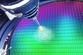
A wafer foundry is a specialized facility that manufactures silicon wafers, the foundational component of semiconductors. These facilities play a critical role in producing integrated circuits (ICs) used in devices like smartphones, laptops, and IoT gadgets. Unlike integrated device manufacturers (IDMs), wafer foundries focus solely on fabrication, enabling cost-effective scaling for consumer electronics companies. The process involves photolithography, etching, and doping to create intricate circuits on silicon substrates. For procurement teams, understanding this supply chain step ensures better vendor negotiations and quality control.
The Development History of Wafer Foundry
The evolution of wafer foundries began in the 1980s, driven by the need to reduce semiconductor production costs. Companies like TSMC pioneered the "pure-play" foundry model, separating design and fabrication. This shift allowed smaller firms to innovate without owning expensive fabrication plants. Over decades, advancements in wafer foundry technology—such as smaller nanometer nodes—enabled higher transistor density and energy efficiency. Today, the industry thrives on collaborations between foundries and consumer electronics giants, ensuring rapid adoption of cutting-edge nodes like 5nm and 3nm.
Key Milestones in Foundry Evolution
1987: TSMC establishes the pure-play foundry model.
2000s: Transition to 300mm wafers boosts productivity.
2020s: Adoption of EUV lithography for sub-7nm processes.
Characteristics of Wafer Foundry
Modern wafer foundries are defined by three core traits: precision, scalability, and adaptability. Precision ensures nanometer-level accuracy in circuit patterning, minimizing defects. Scalability allows mass production of wafers to meet global demand for consumer electronics. Adaptability refers to the ability to support diverse designs, from AI chips to MEMS sensors. Additionally, foundries invest heavily in sustainability, reducing water and energy consumption. For engineering teams, aligning product designs with a foundry’s capabilities is vital for performance and cost efficiency.
Parameters of Wafer Foundry
selecting a wafer foundry requires evaluating technical parameters such as node size, yield rates, and turnaround time. Node size (e.g., 7nm, 5nm) determines transistor density and power efficiency. Yield rates reflect the percentage of defect-free wafers, directly impacting costs. Turnaround time affects time-to-market for new devices. Other factors include:
Wafer size: 200mm vs. 300mm diameters.
Material: Silicon, silicon carbide, or gallium nitride.
Certifications: ISO standards for quality assurance.
Roles of Wafer Foundry in Consumer Electronics
Wafer foundries serve as the backbone of consumer electronics innovation. They transform IC designs into physical chips powering devices like wearables and smart home systems. By offering advanced packaging technologies—such as 3D IC integration—foundries enable slimmer, faster gadgets. Procurement teams rely on foundries to balance cost and performance, especially during component shortages. For example, TSMC’s advanced nodes have been pivotal in producing high-performance processors for leading smartphone brands.
Applications of Wafer Foundry
From smartphones to automotive systems, wafer foundries support diverse applications. In consumer electronics, they produce processors, memory chips, and sensors. Automotive industries depend on foundries for reliable ICs in ADAS and infotainment. Emerging fields like AI and 5G also leverage foundries to create specialized chips. For instance, the rise of edge computing has increased demand for low-power, high-speed wafers. Engineering teams must collaborate closely with foundries to optimize designs for these varied use cases.
Case Study: Smartphone Processors
Leading smartphone brands partner with wafer foundries to develop custom chipsets. Apple’s A-series and Qualcomm’s Snapdragon processors are fabricated using TSMC’s 5nm nodes, enhancing performance and battery life. This collaboration underscores the foundry’s role in delivering competitive advantages.
Manufacturers of Wafer Foundry
The wafer foundry market is dominated by key players like TSMC, Samsung Foundry, and GlobalFoundries. TSMC holds over 50% market share, specializing in advanced nodes. Samsung excels in memory and logic chips, while GlobalFoundries focuses on RF and analog solutions. Regional foundries, such as SMIC in China, are gaining traction amid geopolitical shifts. Procurement teams must assess factors like geopolitical risks, capacity, and technological expertise when selecting a partner.
Conclusion
Understanding wafer foundries is essential for procurement and engineering teams in consumer electronics. From historical milestones to technical parameters, this knowledge drives informed decisions in vendor selection and product design. As the industry advances toward 3nm nodes and beyond, collaboration with top-tier foundries will remain critical for innovation. For further insights, explore authoritative resources like Semiconductor Industry Association.
Inside Chip Design Companies: Innovations Powering Next-Gen Consumer Electronics
2026-09-23
2061
What is a Chip Design Company?
A chip design company specializes in creating integrated circuit (IC) blueprints used in devices ranging from smartphones to AI systems. These firms transform conceptual designs into manufacturable layouts, leveraging tools like electronic design automation (EDA). Unlike semiconductor foundries, chip design companies focus solely on innovation, enabling consumer electronics brands to outsource complex R&D. For procurement teams, partnering with such firms ensures access to cutting-edge technology without heavy upfront investments in design infrastructure.
The Development History of Chip Design Companies
The rise of chip design companies traces back to the 1990s, driven by the need to reduce costs and accelerate innovation. Early pioneers like ARM revolutionized the industry with licensable IP cores, decoupling design from fabrication. This shift allowed smaller firms to compete with giants like Intel. Over time, advancements in EDA tools and Moore’s Law propelled specialization, with companies focusing on niches like GPUs (NVIDIA) or mobile processors (Qualcomm). Today, the sector thrives on collaborations with foundries and OEMs to deliver next-generation chips.
Key Historical Milestones
1990: ARM introduces licensable processor architectures.
2000s: Rise of fabless models, exemplified by Broadcom and MediaTek.
2020s: AI-driven demand for custom ASICs and SoCs.
Characteristics of Chip Design Companies
Modern chip design companies are defined by three pillars: innovation agility, IP portfolio depth, and cross-industry expertise. They rapidly adapt to trends like 5G and edge computing, often releasing updated architectures annually. Robust IP libraries—such as ARM’s Cortex cores—enable reusable designs, reducing time-to-market. Additionally, these firms collaborate with automotive, healthcare, and IoT sectors, tailoring solutions for diverse applications. Engineering teams must evaluate a company’s ability to balance performance, power efficiency, and scalability when selecting a partner.
Parameters of Chip Design Companies
selecting a chip design company requires analyzing technical and operational metrics. Key parameters include:
Node compatibility: Support for 7nm, 5nm, or advanced packaging technologies.
IP diversity: Availability of processor cores, memory controllers, and connectivity modules.
Time-to-market: Average design cycle duration from concept to tape-out.
For example, companies like NVIDIA excel in GPU designs optimized for AI workloads, while Qualcomm dominates mobile SoCs with integrated 5G modems.
Roles of Chip Design Companies in Consumer Electronics
Chip design companies act as innovation engines for consumer electronics. They enable brands to differentiate products through custom silicon, such as Apple’s M-series chips or Google’s Tensor processors. By outsourcing design, OEMs reduce R&D risks and focus on market-specific features. Procurement teams must assess factors like licensing models (royalty-based vs. upfront fees) and long-term roadmap alignment to ensure cost efficiency.
Applications of Chip Design Companies
From smartphones to smart home devices, chip design companies underpin nearly every consumer technology. Key applications include:
Mobile processors: High-performance CPUs for seamless multitasking.
AI accelerators: Specialized chips for machine learning tasks.
IoT controllers: Low-power ICs for connected sensors and wearables.
Emerging fields like quantum computing and autonomous vehicles further expand opportunities for tailored IC solutions.
Case Study: Smartphone Innovation
Apple’s collaboration with chip design companies like TSMC and ARM resulted in the A16 Bionic chip, offering 40% faster GPU performance. This synergy highlights how strategic partnerships drive competitive advantages in crowded markets.
Manufacturers of Chip Design Companies
The chip design company landscape features leaders like NVIDIA, Qualcomm, AMD, and ARM, alongside rising players like MediaTek and Unisoc. NVIDIA dominates AI and graphics, while Qualcomm leads in wireless communication ICs. Regional firms, such as China’s HiSilicon, are gaining traction amid geopolitical shifts. Procurement teams should prioritize partners with proven scalability and geopolitical risk mitigation strategies.
Conclusion
For consumer electronics procurement and engineering teams, understanding chip design companies is vital for strategic sourcing and product development. From historical evolution to technical parameters, this knowledge ensures informed decisions in a rapidly evolving industry. As demand for specialized ICs grows, collaboration with agile design firms will remain critical. Explore authoritative resources like the Semiconductor Industry Association for deeper insights.
Twenty Years Later: Arduino Is Far More Than Just Arduino
2026-09-23
1709
Article Overview
This article explores the evolution of Arduino from an open-source hardware platform to an expanded ecosystem, highlighting its profound impact across multiple domains.
Defining Arduino
Arduino is an open-source hardware and software platform designed to provide a simple, low-cost, yet high-performance entry point into the world of microcontrollers. It was pioneered nearly two decades ago by David Cuartielles, Gianluca Martino, Tom Igoe, David Mellis, and Massimo Banzi.
This definition of Arduino would have sufficed a decade ago. However, Arduino has evolved. Over the past twenty years, thousands of contributors have enriched its open-source ecosystem. Today, Arduino is far more than just Arduino.
How Has Arduino Changed?
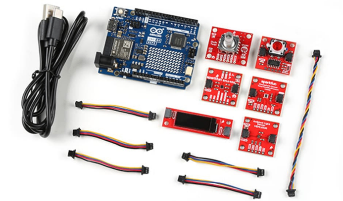
Arduino continues to expand its product lineup. It still offers iterations of the original UNO, along with expanded versions retaining the classic form factor. This includes the UNO R4 with an 8x12 LED matrix, as shown in Figure 1. The new Pro product line features high-performance 32-bit processors and network connectivity, enabling remote monitoring and data sharing. The Pro line also includes Opta, a programmable logic controller (PLC). Enhanced integrated development environments (IDEs) now offer features like a serial plotter.
Figure 1. SparkFun kit showcasing the Arduino Uno R4 and various Qwiic devices.
Where Has Arduino Succeeded?
For many university students and educators, Arduino evokes strong sentiments—from purists who prefer bare-metal programming to enthusiasts who use it for nearly everything. Their consensus? Arduino is a deeply rooted success in global microcontroller communities and makerspaces. In other words, students and hobbyists worldwide are intimately familiar with its hardware and IDE.
But this is not the end of the story, as Arduino’s influence extends far beyond the company and its products.
How Has Arduino Expanded Its Reach?
This is where things get interesting, as we begin to see why our initial definition of Arduino is incomplete. As an engineer at DigiKey, I’ve had the opportunity to explore various platforms. I’ve observed that Arduino has outgrown its original scope. Earlier, I noted that Arduino is nearly a ubiquitous constant in educational settings. This fact hasn’t gone unnoticed—not just by Arduino itself, but also by other manufacturers.
Arduino as a Language Translator
The conversation takes a fascinating turn when shifting focus from Arduino to Raspberry Pi. Here, we encounter diverse technologies. For instance, the Raspberry Pi Pico can be programmed directly from the Arduino IDE. Methods also exist to program the Pi independently while retaining Arduino syntax, a technique applicable to Pi-based PLCs like those from KUNBUS.
Similarly, other manufacturers can import Arduino code into their own IDEs. For example, Microchip’s MPLAB (a DigiKey partner) can import an Arduino project. A sample project might program the UNO, after which the code is ported to MPLAB and deployed to Microchip AVR microcontrollers (originally Atmel). Once again, Arduino’s vast educational foundation is leveraged to deepen understanding of microcontrollers.
Technical Insight:
Massive amounts of Arduino C code have been used to train AI models. Consequently, AI can now assist in generating and optimizing code. For instance, consider non-blocking code generated with AI assistance, as shown in this article. It demonstrates how concepts initially tied to PLC programming can adapt seamlessly to broader applications.

Mastering Chip Etching Machines: Key Insights for Smarter Electronics Manufacturing
2026-09-23
1722
What Is a Chip Etching Machine?
A chip etching machine is a specialized tool used in semiconductor manufacturing to selectively remove material from silicon wafers. This process, known as etching, creates intricate circuit patterns essential for modern electronics. The precision of a chip etching machine ensures components meet exact design specifications, making it indispensable in producing devices like smartphones and computers. Unlike traditional mechanical methods, advanced machines use plasma or chemical reactions for nanoscale accuracy. For example, companies such as Applied Materials and Lam Research dominate this field, offering systems that integrate automation for higher throughput. Learn more about semiconductor processes at Semiconductor Industry Association.
The Development History of Chip Etching Machines
The evolution of chip etching machines mirrors advancements in semiconductor technology. In the 1960s, wet etching dominated, using liquid chemicals to dissolve unprotected silicon. However, the rise of integrated circuits demanded finer control, leading to dry etching techniques like reactive ion etching (RIE) in the 1980s. By the 2000s, plasma-based systems became standard, enabling sub-10nm precision. Today, innovations such as atomic layer etching (ALE) push boundaries further. This progression underscores how chip etching machine capabilities have shaped Moore’s Law, allowing transistors to shrink while performance soars.
Key Milestones
1960s: Introduction of wet etching for early ICs.
1980s: Shift to dry etching for higher precision.
2000s: Plasma etching achieves nanometer-scale accuracy.
2020s: Atomic layer etching (ALE) enables 3D chip architectures.
Characteristics of Chip Etching Machines
Modern chip etching machines are defined by three core traits: precision, scalability, and versatility. Precision ensures minimal material loss, critical for multi-layered chips. Scalability allows adaptation to wafer sizes up to 450mm, meeting mass production demands. Versatility comes from modular designs that support both chemical and plasma etching. For instance, Tokyo Electron’s systems offer configurable gas mixtures to handle diverse materials like silicon, oxides, and metals. These characteristics make chip etching machines vital for fabricating advanced nodes in 5nm and below processes.
Parameters of Chip Etching Machines
selecting a chip etching machine requires evaluating parameters such as etch rate, uniformity, and selectivity. Etch rate determines throughput, while uniformity ensures consistent results across wafers. selectivity—the ability to target specific materials—minimizes damage to underlying layers. Advanced systems also monitor real-time parameters like plasma density and ion energy. For example, ASML’s tools use sensors to adjust conditions dynamically, optimizing performance. These metrics directly impact yield and cost-efficiency, making them critical for procurement teams.
Roles of Chip Etching Machines in Semiconductor Fabrication
In semiconductor manufacturing, chip etching machines serve two primary roles: pattern transfer and material removal. During photolithography, etched patterns define transistor gates and interconnects. Post-deposition, etching removes excess material to isolate components. This dual function ensures chips meet electrical and thermal specifications. As devices shrink, the role of chip etching machines expands to include 3D structuring for memory cells like NAND flash. Such advancements underscore their irreplaceability in cutting-edge fabrication.
Applications of Chip Etching Machines
Chip etching machines are pivotal across industries:
Consumer Electronics: Producing CPUs, GPUs, and memory chips for devices.
Automotive: Fabricating sensors and power management ICs for EVs.
Healthcare: Creating biochips for medical diagnostics.
Emerging applications include quantum computing and flexible electronics, where etching enables novel architectures. For example, Intel uses advanced etching to build stacked transistors for AI accelerators.
Manufacturers of Chip Etching Machines
Leading chip etching machine manufacturers include:
Applied Materials: Known for high-throughput plasma systems.
Lam Research: Specializes in dielectric and metal etching solutions.
Tokyo Electron (TEL): Offers hybrid systems for diverse materials.
These firms invest heavily in R&D to address challenges like edge placement error and line-edge roughness, ensuring their tools meet next-gen demands.
Conclusion
From enabling nanoscale circuits to powering global tech innovation, chip etching machines remain the backbone of semiconductor manufacturing. Procurement and engineering teams must prioritize parameters, applications, and vendor expertise when selecting these systems. As the industry advances toward 2nm nodes and beyond, the role of chip etching machines will only grow more critical.
Function of TVS and the Working Principle & Application of Its Protection Circuit
2026-09-23
2102
This article explores the working principle of TVS diodes and their wide range of applications in fields such as overvoltage protection, ESD protection, and lightning surge protection, revealing their significant value as core components for circuit protection.
How does TVS protect circuits from transient overvoltage impacts?
Working Principle: The TVS diode utilizes the avalanche breakdown characteristic of the p-n junction under reverse bias. When the voltage exceeds the breakdown voltage of the TVS diode, it enters a conductive state and diverts the current to the ground line. This action clamps the transient overvoltage to a safe level, protecting sensitive electronic components. In summary, the TVS diode can clamp transient overvoltage to a safe level within an extremely short time, providing effective protection for electronic circuits. Its fast response and high energy absorption capability make it an ideal choice for overvoltage protection.
Besides overvoltage protection, what other uses do TVS diodes have? Can they be used as interference suppression components in noise suppression circuits?
TVS (Transient Voltage Suppressor) diodes have several other applications besides overvoltage protection and can indeed be used as interference suppression components in noise suppression circuits. Here are several main applications and functions of TVS diodes:
Anti-Electrostatic Discharge (ESD): TVS diodes can effectively absorb high-voltage transient pulses caused by electrostatic discharge, protecting sensitive electronic components from damage. This makes them widely used in computers, communication equipment, consumer electronics, and other fields.
Lightning Strike Protection: In power and signal lines, TVS diodes can be used to prevent transient overvoltage caused by lightning strikes, protecting equipment from damage. This is particularly important for outdoor equipment and communication base stations.
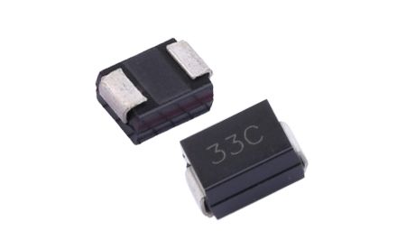
SLKOR TVS diodes P6SMB33CA

Electrostatic Discharge (ESD) Diodes: Invisible Guardians of Circuit Protection
2026-09-23
2125
I. Hazards of ESD and Protection Needs
Electrostatic discharge (ESD) is a phenomenon where charge accumulated on an object’s surface is rapidly released, such as the "electrical shock" feeling when a human touches an electronic device. The voltage released in an instant can reach thousands of volts or higher, causing permanent damage to semiconductor chips. For example, when a static-charged finger touches a phone interface, ESD current may break down the gate oxide inside the chip through the circuit, leading to device failure.
To address this threat, engineers typically deploy ESD protection diodes in circuits. Their core function is to quickly divert current to ground during an ESD event, preventing sensitive components from enduring excessive voltage. Such devices are especially suitable for exposed interfaces like USB, HDMI, and CAN buses—locations most vulnerable to external ESD shocks.
II. Core Working Principles of ESD Diodes
A typical representative of ESD diodes is the Transient Voltage Suppressor (TVS) diode, whose operating mechanism is based on the avalanche breakdown effect of PN junctions:
1. Normal state: The diode is in a high-impedance state and does not affect circuit signal transmission. For example, in USB interfaces, the parasitic capacitance of ESD diodes must be controlled to a few picofarads or lower (e.g., TI’s ESD2CANFD24 is only 2.5pF) to avoid interfering with high-speed data transmission.
2. During ESD impact: When the voltage exceeds the breakdown threshold (e.g., 8kV contact discharge), the diode conducts rapidly, with impedance dropping to near zero, diverting current to ground. At this point, the voltage across the diode is clamped to a safe level (i.e., "clamping voltage"). For instance, ON Semiconductor’s ESD9B5.0ST5G has a clamping voltage of 12.5V at 16A current, protecting backend chips from high-voltage shocks.
3. Recovery characteristics: After the ESD event ends, the diode automatically returns to a high-impedance state, and the circuit resumes normal operation. This process takes only sub-nanoseconds, ensuring signal integrity remains unaffected.
III. Key Technical Parameters and selection Essentials
1. Breakdown Voltage (VBR) and Working Voltage (VRWM)
VRWM is the maximum voltage the diode can withstand during normal operation and must be higher than the circuit signal voltage. For example, if the signal range is 0-3.6V, a device with VRWM ≥ 3.6V should be selected; otherwise, leakage current may occur. VBR is the critical voltage at which the diode starts conducting, typically 10%-20% higher than VRWM.
2. Bidirectional and Unidirectional Structures
● Bidirectional diodes: Have symmetric I-V curves, suitable for bidirectional signals (e.g., HDMI differential lines), protecting against both positive and negative ESD shocks.
● Unidirectional diodes: Allow current to pass in only one direction, ideal for unipolar signals (e.g., USB power lines) and offer better protection against negative voltages. For example, TI’s ESD2CANFD24 features a bidirectional design, optimized for bidirectional communication in automotive CAN buses.
3. Dynamic Resistance (RDYN) and Clamping Voltage
RDYN determines the voltage rise slope during an ESD event. Lower dynamic resistance results in lower clamping voltage and better protection. For example, one ESD diode may have a clamping voltage of 13.4V at 16A current, while another with lower dynamic resistance (as shown in the green TLP curve) has a clamping voltage of only 10V at the same current.
4. Capacitance Characteristics
For high-speed interfaces (e.g., USB3.0), low-capacitance models are required. For instance, ON Semiconductor’s SL15 series reduces capacitance to below 5pF using series compensation diodes, suitable for 5Gbps data transmission.
IV. ESD Protection Industry Standards and Testing
The IEC 61000-4-2 standard developed by the International Electrotechnical Commission (IEC) is the core basis for ESD protection:
● Contact discharge level: Up to 8kV (Level 4), simulating discharge when directly touching equipment.
● Air discharge level: Up to 15kV, simulating static discharge through air gaps.
Notably, there is a difference between a chip’s own ESD rating (e.g., HBM model) and system-level protection requirements. For example, a chip may pass a 2kV HBM test but fail a 2kV IEC test because the IEC model has a faster current rise (<1ns) and higher energy. Therefore, external ESD diodes are necessary to enhance system-level protection.
V. Typical Application Scenarios and Design Recommendations
1. Consumer electronics: USB-C interfaces in phones and tablets typically deploy multi-channel ESD diode arrays (e.g., Dongwo Electronics’ SOT-23 packaged devices) to protect both power and data lines.
2. Automotive electronics: CAN buses require ruggedness; TI’s ESD2CANFD24 supports ±25kV contact discharge, meeting the high reliability needs of in-vehicle systems.
3. Industrial equipment: In RS485 communication lines, low-capacitance ESD diodes (e.g., ESD751’s 0.5pF model) prevent signal distortion.
Design keys:
● Place ESD diodes as close to the interface as possible to shorten the current path.
● Avoid series resistors between the diode and ground to ensure low-impedance discharge.
● For high-frequency signals, balance capacitance and clamping voltage.
VI. Common Misconceptions and Technological Developments
1. Misconception: Assuming a chip’s own ESD rating (e.g., HBM 2kV) is sufficient to protect the system. In reality, the HBM standard only simulates ESD in production environments, while the IEC standard is closer to real-world usage scenarios.
2. Technological trends: As chip integration increases, ESD diodes are moving toward lower capacitance (e.g., 0.1pF) and higher power density (e.g., single-package multi-channel protection). For example, Toshiba’s TVS diodes achieve lower parasitic parameters in QFN packages through optimized wafer processes.
Summary
ESD diodes are the "fuses" of electronic devices. Their design requires comprehensive consideration of circuit characteristics, environmental interference, and industry standards. selecting appropriate ESD protection solutions (e.g., bidirectional/unidirectional structures, low-capacitance models) and strictly following IEC 61000-4-2 testing can significantly improve device reliability and lifespan. Whether in consumer electronics or industrial control, ESD diodes remain "invisible guardians," silently safeguarding the stable operation of modern electronic systems.
About SLKOR:
SLKOR, headquartered in Shenzhen, China, is a rapidly emerging national high-tech enterprise in the power semiconductor sector. With R&D centers in Beijing and Suzhou, its core technical team originates from Tsinghua University. As an innovator in silicon carbide (SiC) power device technology, SLKOR's products are widely used in new energy vehicles, photovoltaic power generation, industrial IoT, and consumer electronics, providing critical semiconductor solutions to over 10,000 clients globally.
The company delivers more than 2 billion units annually, with its SiC MOSFETs and 5th-generation ultrafast recovery SBD diodes setting industry benchmarks in efficiency ratio and thermal stability. SLKOR holds over 100 invention patents and offers 2,000+ product models, continually expanding its IP portfolio across power devices, sensors, and power management ICs. Certifications including ISO 9001, EU RoHS/REACH, and CP65 compliance demonstrate the company's steadfast commitment to technological innovation, lean manufacturing, and sustainable development.
What is the principle of the Hall sensor and what is its use?
2026-09-23
2065
1. What is the Hall Effect?
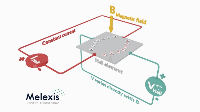
The Hall effect is caused by the interaction between the corresponding electric and magnetic fields of charged particles (such as electrons). For a more vivid and intuitive understanding, you can refer to the animation diagram of the Hall effect principle below.
2. Principle of the Hall Effect
When a conductive plate is connected to a circuit with a battery, current starts to flow. Charge carriers will move along a linear path from one end of the plate to the other. The movement of charge carriers generates a magnetic field. When a magnet is placed close to the plate, the magnetic field of the charge carriers becomes distorted, which disrupts the straight-line flow of the charge carriers. The force that disturbs the direction of the charge carriers' flow is called the Lorentz force.
Due to the distortion of the charge carriers' magnetic field, negatively charged electrons will deflect to one side of the plate, while positively charged holes will deflect to the other side. A potential difference, known as the Hall voltage, will be generated between the two sides of the plate, which can be measured with an instrument.
Hall effect and Lorentz force: the blue arrow B represents the magnetic field passing vertically through the conductive plate
The principle of the Hall effect states that when a current-carrying conductor or semiconductor is introduced into a perpendicular magnetic field, a voltage can be measured at a position perpendicular to the current path.
The Hall voltage, denoted as VH, is given by the formula:
· VH is the Hall voltage on the conductive plate
· I is the current flowing through the sensor
· B is the magnetic field strength
· q is the charge
· n is the number of charge carriers per unit volume
· d is the thickness of the sensor
3. Principle of Hall Effect Sensors
When the magnetic flux density around the sensor exceeds a certain preset threshold, the sensor detects it and generates an output voltage called the Hall voltage (VH). The specific principle is shown in the figure below.
A Hall effect sensor basically consists of a thin rectangular piece of p-type semiconductor material, such as gallium arsenide (GaAs), indium antimonide (InSb), or indium arsenide (InAs), through which a continuous current passes.
Schematic diagram of the Hall effect sensor
When a Hall effect sensor is placed in a magnetic field, the magnetic flux lines exert a force on the semiconductor material, causing charge carriers (electrons and holes) to deflect to either side of the semiconductor plate. This movement of charge carriers is the result of the magnetic force they experience as they pass through the semiconductor material.
As these electrons and holes move sideways, a potential difference is generated between the two sides of the semiconductor material due to the accumulation of these charge carriers. The movement of electrons through the semiconductor material is then affected by an external magnetic field perpendicular to it, and this effect is more pronounced in flat rectangular materials.
The Hall effect provides information about the type of magnetic pole and the magnitude of the magnetic field. For example, a south pole will cause the device to produce a voltage output, while a north pole will have no effect. Typically, Hall effect sensors and switches are designed to be in an "off" state (open-circuit state) when no magnetic field is present. They only "turn on" (closed-circuit condition) when exposed to a magnetic field of sufficient strength and polarity.
4. Hall Effect Sensors
In its simplest form, the sensor operates as an analog sensor, directly returning a voltage. With a known magnetic field, the distance from the Hall plate can be determined. Using a group of sensors, the relative position of the magnet can be inferred.
Usually, Hall effect sensors are combined with circuits that allow the device to operate in digital (on/off) mode, and in this configuration, they may be referred to as switches. The figure below shows a wheel with two magnets passing by a Hall effect sensor.
A wheel with two magnets passing by a Hall effect sensor
Basic Working Principle and Usage Method of Data Converters
2026-09-23
2122
A data converter is an instrument, device, and also an electronic component. Its main function is to convert other types of electrical energy signals into another type, and can convert one type of electrical energy factor signal into another. Data conversion can be divided into two main categories: electrical energy signal conversion and electrical energy factor signal conversion. The following is a detailed introduction by AMEYA360 Electronic Component Purchasing Network: the basic working principle and usage method of data converters.
I. Basic Working Principle of Data Converters
The basic working principle of a data converter is to convert digital signals into analog signals or analog signals into digital signals. Digital signals are represented by binary coding; for example, 8-bit binary coding can convert 256 different levels into digital signals. When converting digital signals to analog signals, the data converter compares the digital signal with a reference voltage and converts the result into an analog signal. Conversely, when converting analog signals to digital signals, the data converter compares the analog signal with a reference voltage and converts the result into a digital signal.
II. Different Types of Data Converters
There are various types of data converters, including:
1. Non-inverting Proportional Amplifier (INA): INA is a basic non-inverting proportional amplifier that converts input signals into output signals, and its amplification factor can be set manually. INA is widely used in data acquisition and amplification systems.
2. Inverting Proportional Amplifier (OTA): OTA is an inverting proportional amplifier that converts input signals into output signals, and its amplification factor can be set manually. OTA is widely used in digital signal processing and digital communication systems.
3. Non-inverting Proportional-Integral Amplifier (INAI): INAI is a non-inverting proportional-integral amplifier that converts input signals into output signals, with a manually set amplification factor, and stabilizes the output signal through an integrator. INAI is widely used in data acquisition and amplification systems.
4. Inverting Proportional-Integral Amplifier (OTAI): OTAI is an inverting proportional-integral amplifier that converts input signals into output signals, with a manually set amplification factor, and stabilizes the output signal through an integrator. OTAI is widely used in digital signal processing and digital communication systems.
5. Dual-Channel Converter (DCD): DCD is a dual-channel converter that converts digital signals to analog signals or analog signals to digital signals. DCD is widely used in digital communication and computer systems.
III. How to Use a Data Converter
A data converter can be used to convert digital signals to analog signals or analog signals to digital signals. The following are simple steps:
(1) Determine the type of data converter to be used.
(2) Configure the data converter to convert digital signals to analog signals or analog signals to digital signals.
(3) Connect the input signal to the input pins of the data converter.
(4) Connect the output signal to an amplifier or send the signal to other devices for further processing.
(5) Measure the output signal of the converter to ensure it meets the expected performance indicators.
Basic Principles of Thyristors
2026-09-23
2150
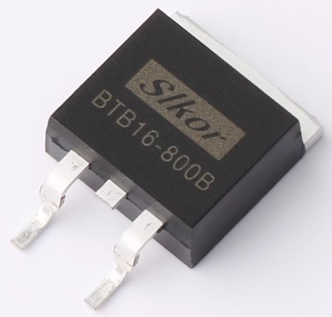
Thyristor conduction conditions: First, a forward voltage must be applied between the anode and cathode of the thyristor; second, a forward voltage must also be applied to the gate. Both conditions must be met simultaneously for the thyristor to enter the conduction state.Slkor BTB16-800B Unidirectional Silicon Control Rectifier SCR TO-263
To put it simply, for a thyristor to conduct:
(1) A signal must be applied;
(2) The anode must be at a higher potential than the cathode (i.e., a forward voltage must exist between them).
Once a thyristor is conducting, it remains conducting even if the gate voltage is reduced or removed. In simple terms, it stays on even when the signal is gone.
Thyristor turn-off conditions: Reduce or remove the forward voltage between the anode and cathode, so that the anode current drops below the minimum holding current.
To simplify:
● For a thyristor to turn on, it needs both a signal and the anode to be at a higher potential than the cathode.
● Once turned on, it stays on even if the signal is removed (a single signal is enough to trigger it).
● To turn it off, either cut off the power supply to the anode-cathode circuit or make the anode potential lower than the cathode potential.
● A unidirectional thyristor is like a controllable diode, with its conduction controlled by a signal. Thus, it allows direct current to pass through unimpeded; for alternating current, it conducts during the positive half-cycle but not the negative half-cycle (the diode here acts as a rectifier).
A bidirectional thyristor (triac) can conduct alternating current.
Case Analysis of Thyristor Control Circuits
Unidirectional Thyristors (Components that can control diodes)Light-Controlled Electronic Switch
● A light-controlled electronic switch uses the conduction and blocking of a thyristor to "turn on" and "turn off". The conduction and blocking of the thyristor are controlled by the intensity of natural light (or artificial light).
● This device is suitable for streetlights, dormitory corridor lights, or lighting in other public places, automatically turning off during the day and on at night to save electricity.
Working principle: As shown in the circuit diagram above:
1. 220V AC is converted into pulsating DC voltage through bulb H and full-bridge rectification, serving as a forward bias (approximately 300V pulsating DC). When this current flows through the diode of the VS unidirectional thyristor to the other end, the bulb lights up. For this to happen, the gate of the thyristor must receive a signal voltage, which requires the 9014 transistor to conduct.
2. How does the 9014 conduct?
The 300V pulsating DC is divided by R1 (100kΩ), R2 (470kΩ), and D (photoresistor). Meanwhile, R1 and DW (zener diode) form a voltage divider, and DW clamps the voltage across R2 and the photoresistor at 6.8V, preparing for the transistor to conduct.
● During the day, when brightness exceeds a certain level, the photoresistor D exhibits a low resistance (≤1kΩ). The entire 6.8V voltage drops across the transistor's base, causing transistor V to cut off (NPN transistors cut off at high levels). No current flows from its emitter, so the unidirectional thyristor VS remains blocked due to the lack of a trigger current, and bulb H does not light. Resistor R1 and zener diode DW limit the transistor's bias voltage to no more than 6.8V, protecting the transistor.
● At night, when brightness falls below a certain level, the photoresistor D exhibits a high resistance (≥100kΩ). This causes transistor V to conduct forward (NPN transistors conduct at low levels), with approximately 0.8V at the emitter, triggering the thyristor VS to conduct and lighting bulb H.
● Installation and Debugging: During installation, place the soldered printed circuit board in a transparent plastic case and secure it. Connect it in series with the controlled light H, and position it to face the sky or a bright area near a building's light-receiving window, avoiding direct exposure to nighttime lights within 3 meters.
● Debugging should be done at dusk. Adjust the resistance of RP so that the controlled light H turns on at an appropriate brightness level.
Simple Delay Lighting
● Circuit principle: The circuit of this delay light is as shown in the attached diagram, with the delay circuit enclosed in the dashed box. In the diagram, K is a switch.
● When K is closed, current flows directly through K to light the bulb, and other circuits remain inactive.
● When K is turned off, the 220V voltage is rectified by the diode. On one hand, it charges capacitor C through R1; during the charging process of C, no current flows through R2, so transistor V remains cut off. On the other hand, this voltage provides a trigger voltage to the thyristor SCR through R3 and R4, keeping the thyristor conducting. Thus, the light stays on for a period after being turned off.
● Once capacitor C is fully charged, current flows through R1 and R2 to the base of transistor V, turning transistor V from cut-off to conduction. When the transistor conducts, current flows through the bulb to R3 and then through the transistor to the negative pole. At this point, because the transistor has low impedance, no current flows through R4 to the thyristor's gate, so the thyristor SCR turns off. Since current flows through the bulb and R3 (220kΩ) has a high resistance, the voltage across the bulb is very low, and the light goes out.
● During the delay period after the light is turned off in this circuit, the delay time is determined by the values of resistor R1 and capacitor C.
● This circuit uses a unidirectional thyristor. During the delay period after the light is turned off, the brightness of the lamp is approximately half of its brightness when it is fully on, which meets people's visual needs while saving energy.
● Circuit production: For the unidirectional thyristor SCR in this circuit, use MCR100-8 with a voltage rating of at least 600V. The bulb power should not exceed 100W. The diode VD is 1N4007, and the transistor V is C1815. All resistors are 1/8W carbon film resistors.
2. Bidirectional Thyristors (Components that can control AC)
The following is a classic bidirectional thyristor circuit, which uses optocoupler isolation to control high-voltage circuits with low-voltage signals, enabling continuous dimming of lights.
What is an operational amplifier?
2026-09-23
1723
An Operational Amplifier (abbreviated as op-amp) is a direct-coupled, differential mode input, typically single-ended output high-gain voltage amplifier. It can generate an output potential (relative to ground) that is hundreds of thousands of times larger than the potential difference at the input. It got its name because it was initially mainly used in analog computing circuits such as addition and subtraction operations.
Working Principle of Operational Amplifier
The differential input of an operational amplifier includes a non-inverting input voltage and an inverting input voltage. An ideal operational amplifier only amplifies the difference between the two voltages, which is called the differential mode input voltage. The output voltage of the operational amplifier is given by the following formula:
Vout = (V+ - V-) * Ado
where Ado is the open-loop differential gain of the operational amplifier.
Ideal Operational Amplifier
An ideal operational amplifier usually has the following characteristics:
1. Infinite open-loop gain (Ado = +∞): An important property of an ideal operational amplifier is that in the open-loop state, the differential signal at the input has an infinitely large voltage gain, which makes the operational amplifier very suitable for adding a negative feedback configuration in practical applications.
2. Infinite input impedance (Zin/Rin = ∞): The input terminals of an ideal operational amplifier do not allow any current to flow in, that is, the current signals at the V+ and V- terminals are always zero, which means the input impedance is infinite.
3. Zero input offset voltage
4. Infinite bandwidth (BW = ∞) with zero phase shift and infinite slew rate: An ideal operational amplifier will amplify input signals of any frequency with the same differential gain, without changing due to the change of signal frequency.
5. Zero output impedance (Zout/Rout = 0): The output terminal of an ideal operational amplifier is a perfect voltage source. No matter how the current flowing to the amplifier load changes, the output voltage of the amplifier remains constant, that is, the output impedance is zero.
6. Zero noise
7. Infinite common-mode rejection ratio (CMRR = ∞): An ideal operational amplifier can only respond to the voltage difference between the V+ and V- terminals, that is, it only amplifies the (V+ - V-) part. The common part of the two input signals (i.e., the common-mode signal) is completely ignored.
8. Infinite power supply rejection ratio
All these idealizations cannot be fully realized. Equivalent resistors and capacitors can be used in the operational amplifier model to simulate the non-infinite or non-zero parameters of a real operational amplifier. In this way, designers can take these influences into account in the overall performance of the final circuit. The impact of some parameters on the final design may be negligible, but other parameters that actually restrict the final performance must be calculated.
Common Application Designs
(1) Inverting Closed-Loop Amplifier
The above figure shows a circuit of an inverting closed-loop amplifier. Assuming this closed-loop amplifier uses an ideal operational amplifier, due to its infinite open-loop gain, the two input terminals of the operational amplifier are virtual ground. Also, because the input impedance is infinite, the current from Vin to V- is equal to the current from V- to Vout, so:
(2) Non-Inverting Closed-Loop Amplifier
The above figure shows a circuit of a non-inverting closed-loop amplifier. The negative feedback determines the closed-loop gain Acl=Vout/Vin through the voltage-divider resistors Rf and Rg. Balance is established when Vout is just sufficient to make the voltage at the inverting terminal equal to Vin. Therefore, the voltage gain of the entire circuit is 1 + Rf/Rg. The output voltage formula is:
(3) Adder
The above figure shows an adder circuit. Under the condition of an ideal operational amplifier, because the input impedance is infinite, the current through R1 is equal to the current through R2, and similarly, the current through R3 is equal to the current through R4. So:
(V1-V+)/R1=(V+-V2)/R2
(Vout-V-)/R3=V_/R4
Also because of virtual short circuit, there is:V+=V_
Then it can be deduced that :Vout=V1+V2
(4) Integrator Circuit
The above figure shows an integrator circuit. Under the condition of an ideal operational amplifier, the open-loop gain is infinite, the voltage at the inverting input terminal is equal to that at the non-inverting terminal, and because the input impedance is infinite, the current through R1 is equal to the current through C1.
The current passing through R1 i=V?/R?
The current passing through C1 i=C·dU./dt
So Vout =((-1/(R?·C?)·fV?dt
The output voltage is proportional to the integral of the input voltage over time, which is why it is called an integrator circuit.
(5) Differentiator Circuit
The above figure shows a differentiator circuit. Under the condition of an ideal operational amplifier, the open-loop gain is infinite, the voltage at the inverting input terminal is equal to that at the non-inverting terminal, and because the input impedance is infinite, the current through R1 is equal to the current through C1.
If V1 is a suddenly applied DC voltage, the output Vout corresponds to a pulse in the opposite direction to V1.
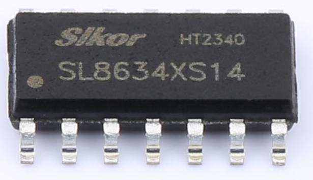
Slkor SL8634XS14 General Op-amp SOP-14
About SLKOR:
SLKOR, headquartered in Shenzhen, China, is a rapidly emerging national high-tech enterprise in the power semiconductor sector. With R&D centers in Beijing and Suzhou, its core technical team originates from Tsinghua University. As an innovator in silicon carbide (SiC) power device technology, SLKOR's products are widely used in new energy vehicles, photovoltaic power generation, industrial IoT, and consumer electronics, providing critical semiconductor solutions to over 10,000 clients globally.
The company delivers more than 2 billion units annually, with its SiC MOSFETs and 5th-generation ultrafast recovery SBD diodes setting industry benchmarks in efficiency ratio and thermal stability. SLKOR holds over 100 invention patents and offers 2,000+ product models, continually expanding its IP portfolio across power devices, sensors, and power management ICs. Certifications including ISO 9001, EU RoHS/REACH, and CP65 compliance demonstrate the company's steadfast commitment to technological innovation, lean manufacturing, and sustainable development.
In-Depth Analysis of DC-DC Switching Regulator Quiescent Current: Definition, Characteristics, and Applications
2026-09-23
1728
Article Overview
In this article, Slkor explores the quiescent current (IQ) of DC-DC switching regulators, covering its definition, measurement conditions, sources, key characteristics, and common misconceptions. Case studies are included to help readers fully understand its critical role in power supply design.
Definition and Measurement Conditions
In DC-DC switching regulators, the quiescent current (IQ) is the self-consumption benchmark of the regulator in a "standby but inactive" state, reflecting the energy consumption level of the IC's internal basic functions.
IQ is defined as the current consumed by the IC under no-load, non-switching, but enabled conditions. Specifically, it is measured under the following criteria:
No Load: No current flows out of the IC's output terminal (e.g., no current at the SW pin of a buck converter or VOUT pin of a boost converter). All current flows internally within the IC to ground.
Non-Switching State: All internal power switches (main switch, control switch, synchronous rectifier) are turned off. The IC enters a high-impedance state, fully disconnecting the power stage from the output (though the MOSFET body diodes in some devices may remain conductive).
Enabled: The IC is activated via the EN pin, is not in an undervoltage lockout (UVLO) or other shutdown state, and power-saving mode must be enabled (if applicable).
Current Sources and Composition
Energy Input Source: The origin of IQ depends on the converter type:
Buck Converter: IQ typically comes only from the input voltage (VIN).
Boost / Buck-Boost Converter: IQ may originate from both VIN and VOUT.
Internal Consumption: IQ powers the IC's essential functions, such as the internal precision reference voltage, oscillator, thermal shutdown circuit, logic gates, etc. It excludes power-stage input current or gate drive current, as these are zero in the non-switching state.
Key Characteristics and Misconceptions
IQ ≠ No-Load Input Current: IQ only reflects the IC's internal "overhead" current. In practical no-load scenarios, the IC must periodically switch to maintain the output voltage (due to leakage losses at the output). The resulting average input current is significantly higher than IQ.
Test Condition Dependency: IQ specifications are valid only under the input/output voltage, temperature, and other conditions specified in the datasheet. Values are not guaranteed outside the recommended operating range.
Summary
IQ is the self-consumption benchmark of a DC-DC switching regulator in a "standby but inactive" state, representing the energy required to sustain its internal basic functions. However, this value does not equate to the actual no-load current in real-world applications. Comprehensive analysis must consider the full system configuration.
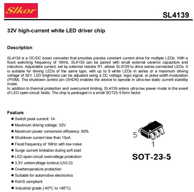
Case Study: SL4139 DC-DC Regulator from Slkor
SL4139 is a DC/DC boost converter that provides precise constant current drive for multiple LEDs. With a fixed switching frequency of 1MHz, SL4139 can be paired with small external ceramic capacitors and inductors. Adjustable current, set by external resistor R1, allows SL4139 to drive series-connected LEDs. It is suitable for driving LEDs of the same type, with up to 9 white LEDs in series or a maximum driving voltage of 32V. LED brightness can be adjusted using a DC voltage, logic signal, or pulse width modulation (PWM). The shutdown control pin (SHDN) enables the device to operate in ultra-low static current standby mode.In addition to thermal protection and overcurrent limiting, SL4139 enters ultra-low power mode in the event of LED open-circuit faults. The chip is packaged in a small SOT23-5 form factor.
About SLKOR:
SLKOR, headquartered in Shenzhen, China, is a rapidly emerging national high-tech enterprise in the power semiconductor sector. With R&D centers in Beijing and Suzhou, its core technical team originates from Tsinghua University. As an innovator in silicon carbide (SiC) power device technology, SLKOR's products are widely used in new energy vehicles, photovoltaic power generation, industrial IoT, and consumer electronics, providing critical semiconductor solutions to over 10,000 clients globally.
The company delivers more than 2 billion units annually, with its SiC MOSFETs and 5th-generation ultrafast recovery SBD diodes setting industry benchmarks in efficiency ratio and thermal stability. SLKOR holds over 100 invention patents and offers 2,000+ product models, continually expanding its IP portfolio across power devices, sensors, and power management ICs. Certifications including ISO 9001, EU RoHS/REACH, and CP65 compliance demonstrate the company's steadfast commitment to technological innovation, lean manufacturing, and sustainable development.
What’s the Difference Between a MOSFET and a Bipolar Transistor?
2026-09-23
1593
When diving into the world of electronics, two types of components you’ll often encounter are MOSFETs (Metal-Oxide-Semiconductor Field-Effect Transistors) and regular transistors. These components are both essential for controlling the flow of electrical current, but they operate in different ways and serve different purposes. Let’s explore the key differences between them.
1. Basic Function
Both MOSFETs and regular transistors (often called BJTs or Bipolar Junction Transistors) are used as switches or amplifiers in electronic circuits. They control the flow of current between two terminals, but they do this in different ways.
MOSFET: The MOSFET is a voltage-controlled device. This means that a small voltage applied to the gate terminal controls the larger current flowing between the source and drain terminals. MOSFETs are widely used in applications where fast switching is required, such as in power supplies and digital circuits.
BJT: A BJT, on the other hand, is a current-controlled device. A small base current controls the larger current flowing between the collector and emitter terminals. BJTs are typically used in applications requiring high current gain, such as in audio amplification and signal processing.
2. Structure and Operation
The internal structure and working principle of a MOSFET and a BJT are quite different.
MOSFET: A MOSFET has three main terminals: Source, Gate, and Drain. The source is where the current enters, and the drain is where it exits. The gate acts as a control terminal and is insulated from the rest of the device, which is why MOSFETs are voltage-controlled. There are two main types of MOSFETs: N-channel and P-channel, depending on the type of semiconductor used in the channel.
BJT: A BJT has three layers of semiconductor material, forming two pn junctions. The layers are called the emitter, base, and collector. A small current at the base controls the current between the collector and emitter. BJTs come in two types as well: NPN and PNP, based on the arrangement of the semiconductor layers.
3. Current vs. Voltage Control
The biggest practical difference between the two is how they are controlled.
MOSFET: As mentioned, MOSFETs are voltage-controlled devices. The voltage applied to the gate terminal creates an electric field that influences the current flow between the source and drain. This makes MOSFETs very energy-efficient, especially in digital circuits, since they require little power to operate the gate.
BJT: BJTs are current-controlled devices. A small current flowing into the base terminal controls the much larger current flowing between the collector and emitter. This means that BJTs are typically more power-hungry when it comes to driving the base, as they need a constant current to operate.
4. Features
Feature
MOSFET
BJT (Bipolar Junction Transistor)
Control Type
Voltage-controlled
Current-controlled
Main Terminals
Source, Gate, Drain
Emitter, Base, Collector
Type of Current Flow
Unidirectional (current flows from source to drain)
Bidirectional (current flows from emitter to collector)
Switching Speed
High (fast switching)
Lower (slower switching)
Power Consumption
Low power consumption (due to voltage control)
Higher power consumption (due to base current)
Efficiency
High efficiency, low heat generation
Less efficient, higher heat generation
Drive Power
Low drive power (no current needed for gate)
High drive power (base current required)
Heat Generation
Low heat generation
Higher heat generation
Speed of Operation
Faster (ideal for high-frequency switching)
Slower (best for analog and low-frequency)
Manufacturing Complexity
More complex to manufacture (due to gate insulation)
Simpler and cheaper to manufacture
Applications
Digital circuits, power supplies, microprocessors, motor control
Audio amplifiers, signal processing, power amplifiers for low-frequency
5. Applications
Both MOSFETs and BJTs have their own unique strengths, and understanding these can help you decide which is best for your application.
MOSFETs are often used in:
Switching power supplies (SMPS)
Microprocessors and digital logic circuits
Motor controllers
Amplifiers for high-frequency applications
BJTs are often used in:
Audio amplifiers
Signal processing circuits
Current amplifiers
Power amplifiers for low-frequency applications
6. Advantages and Disadvantages
Aspect
MOSFET
BJT
Advantages
High efficiency, fast switching, low power consumption, good for high-speed applications
Excellent for high-current applications, simple construction, low cost in some uses
Disadvantages
Sensitive to static discharge, complex to manufacture
Higher power consumption, slower switching, thermal runaway risk
Conclusion
While both MOSFETs and BJTs are integral parts of modern electronics, they differ significantly in how they operate and their ideal applications. MOSFETs are voltage-controlled, highly efficient, and fast, making them perfect for digital circuits and high-speed switching applications. BJTs, on the other hand, are current-controlled and excel in power amplification, especially in low-frequency applications like audio amplifiers.
Understanding the differences between these two types of transistors is crucial when designing circuits to ensure that you choose the best component for the job. Whether you’re working on high-speed digital systems or analog amplifiers, knowing the strengths of each transistor will help you optimize performance and efficiency in your designs.
Invisible Forces, Tangible Electricity: How Do Hall Sensors Work?
2026-09-23
1691
Have you ever wondered why the screen of your laptop turns off when you close the lid? Or why the screen of your smartphone rotates when you flip it over? Or how the motor of an electric vehicle can control its speed so precisely? These phenomena all rely on the work of an unsung hero—the Hall sensor.
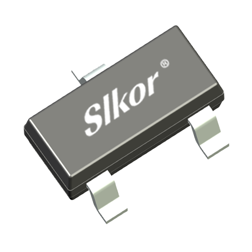
Slkor Hall Sensors
To understand how it works, we need to go back to a physics discovery made over a century ago.
1. The Origin: The Hall Effect—A Classic Physical Phenomenon
In 1879, a young physicist named Edwin Hall made a fascinating discovery during an experiment. He found that when an electric current passes through a thin conductor (or semiconductor) and a magnetic field is applied perpendicular to the current, something unexpected happens.
Let’s use a vivid analogy to help understand:
1. Imagine a highway (the conductor): Electrons are like cars driving at a constant speed, flowing in one direction, creating an electric current.
2. Apply a magnetic field: Now, a strong crosswind (the magnetic field) blows from the side of the highway. This wind pushes all the cars (electrons) as they drive.
3. Voltage Difference is Created: Due to the wind's push, the cars (electrons) shift toward one side of the highway. This causes more cars to gather on one side, while the other side becomes sparse.
4. This is the Hall Voltage: The accumulation of charges generates a voltage between the two sides of the highway, and this is known as the Hall voltage.
Key Takeaway: The Hall effect reveals that when a magnetic field and electric current interact, a voltage proportional to the magnetic field strength is generated across the conductor. The stronger the magnetic field, the greater the Hall voltage.
2. From Phenomenon to Device: The Components of Modern Hall Sensors
Now that we understand the principle, engineers began working on miniaturizing this phenomenon. They used advanced semiconductor technologies (like silicon and gallium arsenide) to integrate the "Hall plate," signal amplifiers, and processing circuits onto a tiny chip smaller than a grain of rice.
Here’s the general process:
1. Sensing: The Hall element (a tiny semiconductor) is exposed to an external magnetic field. When the magnetic field passes through it, it generates a very weak Hall voltage (typically in the microvolt range).
2. Amplification: This raw signal is too weak to be used directly, so an amplifier built into the chip boosts it to a usable level.
3. Processing: Depending on the design, the processing is divided into two main types, corresponding to the two most common types of Hall sensors:
Digital Hall Sensors (Switching/Latched):
Operation: The chip contains a Schmitt trigger (essentially a noise-immune comparator circuit). It compares the amplified voltage to a preset "threshold."
Result: When the magnetic field strength exceeds the "turn-on" threshold, the sensor’s output immediately switches from high to low (or vice versa), like flipping a switch. When the magnetic field weakens below the "turn-off" threshold, the output returns to its original state.
Applications: Contactless switches—For example, lid detection on laptops, car door lights, electric toothbrush activation.
Analog Hall Sensors (Linear):
Operation: The output voltage is directly proportional to the magnetic field strength. The stronger the magnetic field, the higher the output voltage; the weaker the field, the lower the output voltage.
Result: These sensors provide continuous signals, allowing them to detect not only the presence of a magnetic field but also its strength and polarity (north or south).
Applications: Contactless distance, angle, and current measurements—For example, throttle position sensors in cars, joint angle measurement in robotics, and current detection in circuits (by measuring the magnetic field around a live wire, it indirectly calculates the current—very safe).
3. Ubiquitous Applications: Why Do We Love Hall Sensors?
The appeal of Hall sensors lies in their contactless operation, long lifespan, high reliability, and high-frequency response.
Contactless: No physical contact means no mechanical wear, no sparking, and extremely long life—ideal for harsh environments (dust, oil, vibration).
High Speed: They respond incredibly fast, making them perfect for detecting high-speed rotating objects, such as motor speed measurement.
High Accuracy: Linear Hall sensors provide very precise measurements.
As a result, you can find them in a variety of settings:
Consumer Electronics: Automatic screen rotation on phones and tablets; lid detection for Bluetooth earphone cases.
Industrial and Automotive: Motor speed control; piston position detection in cylinders; commutation in brushless motors; current monitoring in battery management systems.
Home Appliances: Drum speed measurement in washing machines; flow measurement in water purifiers.
Conclusion
From the pure physics discovery in 1879 to the smart "sensors" embedded in billions of devices today, Hall sensors perfectly demonstrate how basic science can drive technological revolutions. They act as a bridge, turning invisible, intangible magnetic fields into precise electrical signals that electronic systems can understand and use. The next time your phone screen lights up as you rotate your wrist, you can smile, knowing that the brilliance of Dr. Hall and countless engineers is quietly working behind the scenes to serve you.
Introduction to MOSFET SOT-23 Package
2026-09-23
1353
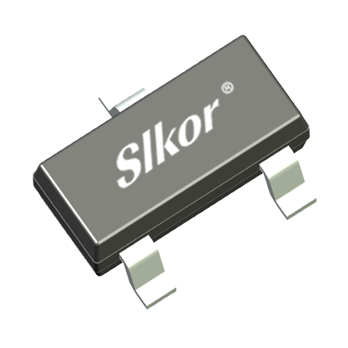
The SOT-23 is a very common and widely used surface-mount semiconductor package, particularly suited for low-power transistors (including MOSFETs, BJTs), diodes, and integrated circuits.
1. SOT-23 Package Overview
Full Name: Small Outline Transistor 23
Type: Surface-mount device
Features: Small size, low cost, suitable for high-density PCB installations.
Main Applications: Consumer electronics, mobile phones, laptops, portable devices, and other applications where space is crucial.
2. Package Structure and Physical Characteristics
Shape and Size:
The package is a rectangular plastic body. Typical dimensions are very small, approximately 2.9mm in length, 1.3mm in width, and 1.0mm in height. These compact dimensions make it occupy minimal space on the PCB.
Pin Count and Arrangement:
The most common version is a 3-pin package (SOT-23-3), which is the preferred configuration for MOSFETs.
There are also variants with 5 pins (SOT-23-5) or 6 pins (SOT-23-6), used for ICs with multiple transistors or an enable pin.
The pins typically extend outward in a "gull-wing" shape, making soldering and inspection easier.
Pinout Example (for a 3-pin N-MOSFET):
Pin 1 (Source): Source terminal.
Pin 2 (Gate): Gate terminal.
Pin 3 (Drain): Drain terminal.
Important Note: Pin definitions may vary between manufacturers! Always consult the datasheet for the specific part number to verify the pinout. Common pinouts include G-D-S and S-G-D.
The diagram below illustrates a typical SOT-23 package size and pin arrangement:
3. SOT-23 MOSFET Characteristics and Performance
Due to its tiny size, the SOT-23 packaged MOSFET has clear positioning and limitations in terms of performance:
Advantages:
Compact: The primary advantage, saving valuable PCB space.
Low Cost: With minimal packaging materials and mature manufacturing processes, SOT-23 MOSFETs are highly cost-effective.
Lightweight: Ideal for portable devices.
Good High-Frequency Performance: Short pins and low parasitic inductance make it suitable for high-frequency switching applications.
Disadvantages and Limitations:
Limited Power Handling: The primary limitation. Due to its small size, it has poor heat dissipation.
Relatively High On-Resistance: Due to the small die size, the on-resistance tends to be higher compared to larger MOSFET packages.
Low Current Handling: Typically, it can only handle continuous currents ranging from a few hundred milliamps to 1-2A.
4. Typical Applications
SOT-23 MOSFETs are typically used in low-power switching and control circuits, such as:
Load Switching: Control the power supply to a circuit module.
Level Shifting: Convert logic levels between different voltages.
Signal Switching: Switch analog or digital signals.
Motor Driving: Drive very small DC motors (e.g., toy motors).
LED Driving: Control small current LEDs.
5. selection and Usage Considerations
Verify Pinout: Again, it's crucial to consult the datasheet to confirm the pinout, as it can vary by manufacturer.
Thermal Performance:
Pay attention to the maximum power dissipation and the thermal resistance from junction to ambient in the datasheet. If the power dissipation is high, copper traces on the PCB should help with heat dissipation, and if a heatsink is present, ensure it is connected to the thermal pad.
Check Electrical Parameters:
Vds (Drain-Source Voltage) and Vgs (Gate-Source Voltage) should meet the required voltage ratings.
Id (Continuous Drain Current) should meet the circuit’s current requirements with some margin.
Rds(on) (On-Resistance) should be low to minimize conduction losses.
Soldering Considerations:
For manual soldering, use a fine-tipped soldering iron and be careful to avoid solder bridges between pins.
Reflow soldering is the most common method for mass production.
Summary
Characteristic
Description
Full Package Name
Small Outline Transistor 23
Main Features
Small size, low cost, suitable for high-density mounting
Typical Dimensions
2.9mm x 1.3mm x 1.0mm
Common Pin Count
3 pins (SOT-23-3)
Advantages
Compact, inexpensive, lightweight, good high-frequency performance
Disadvantages
Poor heat dissipation, limited power, low current, high on-resistance
Applications
Portable devices, low-power switches, level shifting, signal switching
Key selection Factors
Pinout, voltage ratings, current, on-resistance, thermal performance
In conclusion, the SOT-23 is one of the most basic and commonly used packages in an electronic engineer's "package library." When you need a small, low-cost switch to handle signals or control low-power loads, it's often the go-to choice. However, when dealing with significant power handling, a larger MOSFET package should be considered.
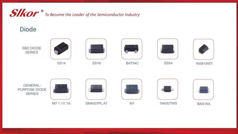
Do You Know These Twenty Types of Diodes?
2026-09-23
1265
Detector Diode
The main function of a detector diode is to extract the low-frequency signal from a high-frequency signal. They are constructed with a point-contact structure, which means they have a small junction capacitance and can operate at high frequencies. Typically, they are made of germanium material. In principle, the process of extracting the modulating signal from the input signal is called detection. With a rectification current of 100 mA as the boundary, those with an output current less than 100 mA are referred to as detector diodes. Germanium point-contact type diodes can operate at frequencies up to 400 MHz, with low forward voltage drop, small junction capacitance, high detection efficiency, and good frequency characteristics, such as the 2AP type. In addition to detection, these diodes can also be used in circuits for limiting, clipping, modulating, mixing, switching, and other functions. There are also special combinations of two diodes with consistent characteristics for FM detection.
Rectifier Diode
In principle, the process of obtaining a direct current (DC) output from an alternating current (AC) input is called rectification. With a rectification current of 100 mA as the boundary, those with an output current greater than 100 mA are referred to as rectifier diodes. They have a planar structure, resulting in a larger junction capacitance and are generally used below 3 kHz. The maximum reverse voltage ranges from 25 volts to 3000 volts, divided into 22 grades from A to X. They are classified as follows: ① Silicon semiconductor rectifier diodes (2CZ type), ② Silicon bridge rectifiers (QL type), and ③ High-voltage silicon stacks used in television sets with a working frequency close to 100 kHz (2CLG type).
Clipping Diode
When a diode is forward-biased and conducts, its forward voltage drop remains essentially constant (0.7 V for silicon diodes and 0.3 V for germanium diodes). This characteristic is utilized in circuits as a clipping element to limit the signal amplitude within a certain range. Most diodes can be used for clipping. There are also specialized clipping diodes, such as those for protecting instruments and high-frequency Zener diodes. To enhance the ability to limit sharp amplitude spikes, silicon diodes are commonly used. Components are also available that consist of several rectifier diodes connected in series to form a single unit based on the required clipping voltage.
Modulating Diode
This typically refers to diodes specifically used for ring modulation, which are combinations of four diodes with consistent forward characteristics. Although other varactor diodes also have modulation applications, they are usually used directly for frequency modulation.
Mixing Diode
When using diode mixing methods, in the frequency range of 500 Hz to 10,000 Hz, Schottky and point-contact diodes are commonly used.
Amplifying Diode
Amplification using diodes generally involves negative resistance devices such as tunnel diodes and bulk-effect diodes, as well as parametric amplification using varactor diodes. Therefore, amplifying diodes usually refer to tunnel diodes, bulk-effect diodes, and varactor diodes.
Switching Diode
A diode has a very low resistance when forward-biased and is in a conducting state, similar to a closed switch; when reverse-biased, it has a very high resistance and is in a cutoff state, similar to an open switch. The switching characteristics of diodes can be used to form various logic circuits. There are switching diodes used for logic operations with small currents (around 10 mA) and those used for core excitation with currents in the hundreds of milliamperes. Small-current switching diodes are typically point-contact and key-type diodes, while silicon diffusion, mesa, and planar diodes are also available for use in high-temperature environments. The main advantage of switching diodes is their fast switching speed. Schottky diodes have particularly short switching times and are ideal switching diodes. The 2AK type point-contact diodes are used for medium-speed switching circuits, while the 2CK type planar diodes are used for high-speed switching circuits. They are also used in switching, limiting, clamping, or detection circuits. Schottky (SBD) silicon high-current switching diodes have low forward voltage drop, fast speed, and high efficiency.
Varactor Diode
Varactor diodes are small-power diodes used for automatic frequency control (AFC) and tuning. They are also known by various names among Japanese manufacturers. By applying a reverse voltage, the junction capacitance of the diode changes. Therefore, they are used in applications such as automatic frequency control, scanning oscillation, frequency modulation, and tuning. Typically, they are made of silicon using a diffusion process, but other special types such as alloy diffusion, epitaxial junction, and double-diffusion diodes are also used because these diodes exhibit a particularly large change in capacitance with voltage. The junction capacitance varies with the reverse voltage VR, replacing variable capacitors and used in tuning circuits, oscillator circuits, and phase-locked loops. They are commonly used in television high-frequency heads for channel conversion and tuning circuits and are mostly made of silicon.
Frequency Multiplier Diode
For frequency multiplication using diodes, there are two types: frequency multiplication using varactor diodes and frequency multiplication using step (or abrupt) recovery diodes. Varactor diodes used for frequency multiplication are called variable reactance diodes. Although the working principle of variable reactance diodes is the same as that of varactor diodes used for automatic frequency control, the construction of reactance diodes can handle higher power. Step recovery diodes, also known as step recovery diodes, have a short reverse recovery time trr when switching from conduction to cutoff. Therefore, their main advantage is the significantly short transfer time when rapidly switching to the cutoff state. If a sinusoidal wave is applied to a step recovery diode, due to the short transfer time tt, the output waveform is sharply truncated, resulting in the generation of many high-frequency harmonics.
Zener Diode
This type of diode is made using the reverse breakdown characteristic of a diode, maintaining a nearly constant voltage across its terminals to stabilize the voltage in a circuit. It is a product that replaces voltage stabilizing electronic diodes. It is a diode with a steep reverse breakdown characteristic curve. It is used as a control voltage and reference voltage. The diode's operating voltage (also known as Zener voltage) ranges from around 3 V to 150 V, with many grades divided by 10%. In terms of power, products are available from 200 mW to over 100 W. Operating in the reverse breakdown state, made of silicon material, with a very small dynamic resistance RZ, typically 2CW, 2CW56, etc.; two complementary diodes connected in reverse series to reduce the temperature coefficient are 2DW type.
The temperature coefficient α of a Zener diode: α represents the change in the stabilization voltage per 1°C temperature change. Diodes with a stabilization voltage less than 4 V have a negative temperature coefficient (due to Zener breakdown), meaning the stabilization voltage decreases with increasing temperature (temperature causes valence electrons to move to higher energy levels); diodes with a stabilization voltage greater than 7 V have a positive temperature coefficient (due to avalanche breakdown), meaning the stabilization voltage increases with increasing temperature (temperature increases atomic vibration amplitude, hindering carrier movement); diodes with a stabilization voltage between 4 and 7 V have a very small temperature coefficient, nearly zero (both Zener and avalanche breakdowns occur).
PIN Diode
This is a crystal diode constructed with an intrinsic semiconductor (or a semiconductor with low impurity concentration) sandwiched between the P and N regions. The "I" in PIN stands for "intrinsic." When operating at frequencies above 100 MHz, due to the storage effect of minority carriers and the transit time effect in the "intrinsic" layer, the diode loses its rectifying action and becomes an impedance element, with its impedance value changing with the bias voltage. In zero bias or reverse bias, the impedance of the "intrinsic" region is very high; in forward bias, due to the injection of carriers into the "intrinsic" region, the "intrinsic" region exhibits a low impedance state. Therefore, a PIN diode can be used as a variable impedance element. It is commonly used in high-frequency switching (microwave switching), phase shifting, modulation, limiting, and other circuits.
Avalanche Diode
This is a transistor that can generate high-frequency oscillations under the influence of an applied voltage. The working principle of generating high-frequency oscillations is as follows: using avalanche breakdown to inject carriers into the crystal, since the transit time of carriers across the wafer is finite, the current lags behind the voltage, resulting in a delay time. If the transit time is appropriately controlled
Tunnel Diode
The tunnel diode is a crystal diode whose primary current component is the tunneling current. Its base materials are gallium arsenide and germanium. The P-type and N-type regions are highly doped (i.e., with high concentrations of impurities). The tunneling current is generated by the quantum mechanical effects of these degenerate semiconductors. The occurrence of the tunneling effect requires the following three conditions: ① The Fermi level is located within the conduction band and the valence band; ② The space charge layer must be very narrow (less than 0.01 micrometers); there is a possibility of overlap between the energy levels of holes in the P-type region and electrons in the N-type region of the degenerate semiconductor. The tunnel diode is a two-terminal active device. Its main parameter is the peak-to-valley current ratio (IP/PV), where the subscript "P" represents "peak" and the subscript "V" represents "valley." The tunnel diode can be used in low-noise high-frequency amplifiers and high-frequency oscillators (with operating frequencies reaching the millimeter wave band) and can also be used in high-speed switching circuits.
Step Recovery Diode
This is also a diode with a PN junction. Its structural feature is a steep impurity distribution at the PN junction boundary, forming a "self-sustaining electric field." Since the PN junction conducts with minority carriers under forward bias and has a charge storage effect near the PN junction, the reverse current requires a "storage time" to drop to its minimum value (the reverse saturation current value). The "self-sustaining electric field" of the step recovery diode shortens the storage time, allowing the reverse current to cut off quickly and produce rich harmonic components. These harmonic components can be used to design comb spectrum generation circuits. The step recovery diode is used in pulse and higher-order harmonic circuits.
Schottky Barrier Diode
This is a diode with a "metal-semiconductor junction" that exhibits Schottky characteristics. It has a low forward voltage drop. The metal layer can be made of materials such as gold, molybdenum, nickel, and titanium. The semiconductor material is typically silicon or gallium arsenide, usually in the form of N-type semiconductors. This device conducts with majority carriers, so its reverse saturation current is much larger than that of a PN junction, which conducts with minority carriers. Since the storage effect of minority carriers in Schottky diodes is minimal, its frequency response is limited only by the RC time constant, making it an ideal device for high-frequency and fast switching applications. Its operating frequency can reach up to 100 GHz. Additionally, MIS (metal-insulator-semiconductor) Schottky diodes can be used to make solar cells or light-emitting diodes. It can also serve as a freewheeling diode, providing freewheeling function in inductive loads such as inductors in switch-mode power supplies and relays.
Damping Diode
Damping diodes are commonly used in high-frequency voltage circuits. They have a high reverse working voltage and peak current, with a low forward voltage drop. These high-frequency, high-voltage rectifier diodes are used for damping and voltage boosting in the horizontal scanning circuit of televisions. Common damping diodes include 2CN1, 2CN2, and BSBS44.
Transient Voltage Suppression Diode
The TVP diode provides rapid overvoltage protection for circuits. It is available in both bipolar and unipolar types, classified by peak power (500W - 5000W) and voltage (8.2V - 200V).
Double-Base Diode (Single-Crystal Transistor)
This is a three-terminal negative resistance device with two bases and one emitter. It is used in relaxation oscillator circuits and timing voltage readout circuits. It has the advantages of easy frequency adjustment and good temperature stability.
Light-Emitting Diode (LED)
Made of gallium phosphide and gallium arsenide phosphide materials, these LEDs are small in size and emit light when forward-biased. They operate at low voltage and current, with uniform light emission, long life, and the ability to emit red, yellow, green, and blue monochromatic light. With technological advancements, white high-brightness LEDs have been developed, giving rise to the emerging LED lighting industry. They are also used in displays for VCDs, DVDs, calculators, and other devices.
Silicon Power Switching Diode
The silicon power switching diode has the capability for high-speed conduction and cutoff. It is primarily used in high-power switching or voltage stabilizing circuits, DC converters, high-speed motor speed control, and as a high-frequency rectifier and freewheeling clamp in drive circuits. It has the advantages of soft recovery characteristics and strong overload capacity, and is widely used in computer power supplies, radar power supplies, and step motor speed control applications.

Find a switching diode – get to know the Slkor Micro 1N4148W
2026-09-23
1237
In electronic product design, a single small diode can often significantly impact the overall power consumption, heat dissipation, and signal quality of the device. The 1N4148W switching diode, launched by Slkor Semiconductor, is specifically designed to address these practical challenges. This product features a SOD-123 package and offers characteristics such as fast switching response, low forward voltage drop (VF), and low reverse leakage current (IRM), enabling effective power consumption control while ensuring signal integrity.
1N4148W: Performance Specifications, Product Features, and Application Fields
The Slkor 1N4148W is a general-purpose small-signal switching diode featuring a reverse recovery time of just 4 ns, a forward voltage drop as low as 1.0 V, and a reverse leakage current of 25 nA. The SOD-123 surface-mount package offers a compact board footprint and lightweight design, making it ideal for automated assembly lines and ensuring high soldering reliability. With an operating junction temperature range of-65°C to +150°C, this diode meets the diverse application requirements of switching power supplies, industrial control systems, and consumer electronics.
Core Parameters
Reverse Repeat Peak Voltage (VRRM): 75 V;
Forward average current (IO): 150 mA;
Forward voltage drop (VF): 1.0 V;
Reverse leakage current (IRM): 25 nA;
Reverse recovery time (Trr): 4 ns;
Dissipated power (Pd): 410 mW;
Operating temperature range: -65°C to +150°C.
Product Features
High conductivity with low conduction loss;
Fast switching speed – reverse recovery time of just 4 ns;
Surface-mount package, ideal for automated placement;
Suitable for general-purpose switching applications;
The plastic material meets the UL-approved flame retardancy rating of 94V-O.
Slkor 1N4148W Product Specification Sheet
Primary Application Areas
Consumer electronics: smart door locks, wearable watches, Bluetooth earbuds, portable blood oxygen saturation monitors, etc.;
Industrial control: sensor signal isolation, optocoupler driving, gate protection, relay current continuity, etc.;
Computers and peripherals: the signal control section for motherboards, graphics cards, keyboards, routers, and power adapters.
Product ID
Manufacturer Model
specifications
Brand Name
category
C444720
1N4148W
SOD-123
Slkor (Slkorwei)
switching diode
About Slkor
Shenzhen Slkor Microelectronics Co., Ltd. was founded in 2015 by Mr.Song Shiqiang in Huaqiangbei, Shenzhen. Initially focused on the research, development, and manufacturing of power devices such as silicon carbide MOSFETs and IGBTs, the company has now expanded its product portfolio to include TVS (Transistor-Transistor-Schottky) static protection diodes, Schottky diodes and transistors, as well as the R&D and manufacturing of analog chips—including power management solutions, Hall sensors, and operational amplifiers. The company's core technical team comprises professionals from Yonsei University and Tsinghua University in South Korea. Slkor has obtained certifications including ISO9001, ISO14001, California Proposition 65 compliance, RoHS, and REACH; it maintains a robust quality management system and ensures stable, reliable delivery. Guided by the philosophy "Slkor: Driving the Future with Microelectronics," the "Slkor" brand has provided products and supporting technical services to tens of thousands of customers worldwide. The company's vision is to become an internationally influential and competitive semiconductor enterprise!





 粤公网安备44030002007346号