Service Hotline
BTA41-800B TRIAC:40A High-Current AC Phase-Control Thyristor (TO-3P)
2026-08-28
311
General Description
In high-power home appliances, industrial AC voltage regulation, motor speed control and heating load control circuits, the TRIAC serves as a contactless AC switch. Its voltage withstand capability, current-carrying capacity, triggering stability and thermal performance directly determine overall system reliability.
The Slkor BTA41-800B is a four-quadrant bidirectional thyristor (TRIAC) in a TO-3P power package. It features an 800V repetitive peak off-state voltage, 40A RMS on-state current, a maximum gate trigger current of 50mA and a gate trigger voltage of 1.5V. Supporting bidirectional AC conduction with excellent thermal dissipation, it is a cost-effective domestic choice for medium-to-high-power AC switching and phase-control applications.
Key Specifications
Repetitive peak off-state voltage (VDRM): 800V
RMS on-state current (IT(RMS)): 40A
Maximum gate trigger current (IGT): 50mA
Gate trigger voltage (VGT): 1.5V
Package: TO-3P
Product Advantages
1. 800V High Voltage Withstand for Mains Applications
With an 800V off-state voltage rating, the device reliably handles mains surges and voltage spikes, reducing the risk of high-voltage breakdown. It is well suited for 220V AC grid systems in home appliances and industrial control equipment.
2. 40A High Current-Carrying Capacity for Heavy Loads
The 40A RMS on-state current enables it to drive high-power heating elements, AC motors and other heavy loads, meeting the current demands of water heaters, high-power temperature-control equipment and motor drives. It offers strong load-handling capability and excellent surge resistance.
3. Friendly Triggering Conditions, Simple Control Circuitry
With a typical gate trigger voltage of 1.5V and a maximum trigger current of 50mA, the device can be directly driven by conventional MCUs and optocouplers without complex peripheral drive circuitry, simplifying hardware design. Four-quadrant triggering ensures reliable conduction in both positive and negative half-cycles, delivering balanced and stable AC waveform control.
4. TO-3P Power Package with Superior Thermal Dissipation
The standard TO-3P power package supports direct heatsink mounting with low thermal resistance, keeping temperature rise under control during continuous high-power operation. It is easy to assemble and compatible with industry-standard footprints, enabling direct replacement of imported TRIACs of the same type.
5. Mature Process with High Batch Consistency
Backed by Slkor's mature thyristor manufacturing process, the device delivers strong commutation capability, excellent dV/dt immunity, low batch-to-batch parameter variation and strong anti-interference performance — ideal for high-volume production of home appliances and industrial equipment.
Applications
Widely used in AC phase control and contactless switching:
Instantaneous electric water heaters
High-power heater temperature control
AC motor speed regulation
Dimming and power-regulation circuits
Solid-state relays (SSRs)
Washing machines and high-power small home appliances
Industrial voltage-regulation modules
Fan and pump control
Lighting power adjustment
Engineering Design Recommendations
Thermal Design: A properly rated heatsink must be matched for 40A high-current operation to control junction temperature and prevent overheating damage.
Drive Circuit: Add a current-limiting resistor in the gate loop to keep the trigger current within a reasonable range, preventing gate overcurrent damage.
Inductive Loads: When driving motors, transformers and other inductive loads, add an RC snubber circuit to suppress voltage spikes and prevent false triggering.
PCB Layout: Widen main power traces to reduce high-current loop impedance; separate power loops from weak trigger signal traces to minimize interference.
Summary
The Slkor BTA41-800B TRIAC combines an 800V voltage rating, 40A on-state current and a TO-3P high-power package. With simple and reliable triggering, it targets 220V AC high-power loads and is suitable for heating, motor speed control, AC switching and various phase-control circuits — making it a preferred domestic thyristor device for high-power home appliances and industrial control.BTA41-800B To Product Pag
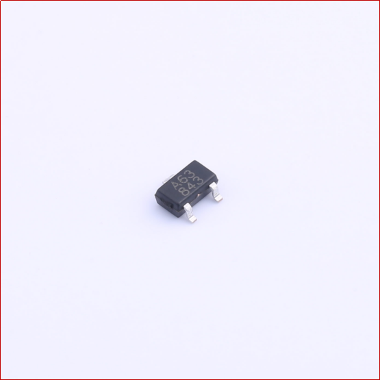
SL1303SE Omnipolar Hall Sensor :Nanoamp Ultra-Low Power Magnetic Detection Switch
2026-08-27
431
For TWS Bluetooth headsets, wearable devices, IoT terminals and battery-powered portable products, non-contact magnetic detection imposes strict requirements on sensor standby power consumption, assembly convenience and miniaturization. The SL1303SE is an omnipolar micro-power Hall magnetic sensor developed by Slkor Semiconductor. Adopting an intermittent scanning detection mechanism, it achieves an ultra-low average operating current of 160nA. Triggered by both N-pole and S-pole magnets without polarity identification, it is packaged in a compact SOT-23-3L form factor. It serves as a cost-effective domestic sensor solution for magnetic switch detection and position judgment in battery-powered products.
1. Core Electrical Parameters
Polarity: Omnipolar (N/S pole both triggerable) Supply Voltage (VDD): 5.5V Average Operating Current (IDD): 160nA Scanning Frequency: 50Hz Package: SOT-23-3L
2. Core Product Advantages
2.1 Omnipolar Induction Simplifies Production Assembly
As an omnipolar switching sensor, the SL1303SE can trigger signal output whether approached by an N-pole or S-pole magnet. There is no need for strict magnetic pole calibration during product assembly, which greatly reduces production difficulty and defect rates. It is highly suitable for mass manufacturing of consumer electronic products.
2.2 Nanoamp-level Ultra-Low Power Extends Battery Life
The chip adopts a periodic sleep-scan operating mode. At a 50Hz scanning frequency, the typical operating current is only 160nA with extremely low static power consumption. It effectively minimizes standby power loss of the whole device and significantly prolongs the service life of products powered by button batteries and small lithium batteries, perfectly adapting to long-standby IoT and portable hardware.
2.3 Compact SOT-23-3L Package Saves PCB Space
Packaged in industry-standard SOT-23-3L surface-mount package, the sensor features tiny size and excellent SMT compatibility. It fits electronic devices with compact PCB layout and supports product thinning and miniaturization design. With stable supply, it is ideal for mass replacement and project selection.
2.4 50Hz Scanning Frequency Optimized for Low-Speed Detection
The 50Hz sampling scanning rate is specially optimized for low-speed magnetic detection scenarios such as switch opening/closing and position recognition. Balancing ultra-low power consumption and detection reliability, it stably identifies the approaching and departing states of magnets and outputs clean and stable signals.
2.5 Mature Process with Excellent Batch Consistency
Based on Slkor’s mature semiconductor manufacturing process, the chip features stable trigger threshold, strong anti-interference capability and wide voltage adaptability, matching mainstream supply voltage of consumer electronics. It can directly replace imported omnipolar ultra-low-power Hall sensors with equivalent specifications.
3. Main Application Fields
The SL1303SE is widely applied in various battery-powered electronic products, including TWS headset cover opening detection, laptop and tablet flip magnetic detection, smart lock position sensing, door magnetic switches, wearable devices, smart toys, flow meters, small home appliance magnetic switches, low-power IoT terminals and other non-contact position detection scenarios.
4. Engineering Design Guidelines
Power Supply Design: The maximum rated supply voltage is 5.5V. Add a 0.1μF decoupling capacitor near the power pin for filtering to suppress power noise and ensure stable operation.
Power Consumption Characteristics: The device works in intermittent scanning mode with a fixed 50Hz frequency. It is not applicable for high-speed magnetic field changes and is only recommended for low-speed position and switch detection applications.
Magnet Matching: Select a reasonable magnetic field strength to ensure the magnetic field reaches the trigger threshold when the magnet approaches. Excessive distance will cause detection failure.
PCB Layout: Keep the sensor away from high-current coils and strong magnetic components to avoid false triggering caused by external magnetic interference. Simplify wiring to reduce parasitic disturbance.
5. Product Summary
The Slkor SL1303SE is a high-performance omnipolar Hall sensor integrating omnipolar triggering, 160nA nanoamp-level ultra-low power consumption, 50Hz fixed scanning frequency and compact SOT-23-3L package. It eliminates magnetic pole identification requirements, greatly simplifies assembly procedures, and focuses on non-contact magnetic detection for battery-powered devices. With stable performance and cost advantages, it is the preferred domestic magnetic switching device for Bluetooth headsets, wearable devices and low-power IoT hardware.SL1303SE To Product Pag
IRLML6402 P-Channel Low-Voltage MOSFET : SOT-23 High-Current Low-Resistance Premium Switching Device
2026-08-26
560
In circuits such as portable consumer electronics, battery management systems, miniature motor drives, and smart home control modules, high-side power switches and load on-off control impose strict requirements on MOSFET conduction loss, current carrying capacity and switching response speed. The Slkor IRLML6402 is a P-channel enhancement-mode low-voltage MOSFET packaged in standard SOT-23. It features 20V withstand voltage, 3.7A continuous current and ultra-low on-resistance of 65mΩ, balancing excellent high-current processing capability and minimal conduction loss. It serves as a cost-effective domestic alternative ideal for high-side switching, battery anti-reverse connection and power path control scenarios.
1. Core Electrical Parameters
Device Type: P-Channel Enhancement Mode MOSFET Package: SOT-23 Drain-Source Breakdown Voltage (VDSS): 20V Continuous Drain Current (Id): 3.7A On-Resistance (RDSON): 0.065Ω @ -4.5V, -3.7A Gate Threshold Voltage (VTH): -1.2V @ -250μA
2. Core Product Advantages
2.1 Standard SOT-23 Package for Automated Production
Packaged in industry-standard SOT-23 surface-mount form factor, the IRLML6402 occupies minimal PCB space and features excellent SMT compatibility. It supports automated mass production and is widely adopted in space-limited circuit boards and portable device modules, achieving a perfect balance between product miniaturization and mass-production efficiency.
2.2 Ultra-Low On-Resistance Reduces High-Current Loss
With an ultra-low on-resistance of only 65mΩ at a gate driving voltage of -4.5V, the device stably supports 3.7A continuous operating current. It generates less heat under heavy-load conditions, effectively reducing circuit power consumption and temperature rise, and improving overall equipment efficiency and battery endurance.
2.3 P-Channel High-Side Drive Simplifies Power Control Circuits
As a P-channel MOSFET, it can be directly used for positive power high-side switching, realizing high-side load control, power anti-reverse protection and battery charge-discharge path switching. It eliminates the need for complex level conversion circuits and simplifies peripheral design compared with N-channel solutions requiring bootstrap drive, effectively reducing BOM cost.
2.4 Fast Switching Response and Strong Working Adaptability
The device delivers fast switching speed and stable threshold voltage characteristics with excellent anti-interference performance, making it suitable for frequent load switching scenarios. It supports a wide operating temperature range and fully meets the application requirements of consumer electronics and partial industrial environments.
2.5 Mature Domestic Process with Consistent Batch Quality
Adopting Slkor’s mature trench semiconductor process, the IRLML6402 features minor parameter deviation between batches, ultra-low leakage current and outstanding impact resistance. It can directly replace imported mainstream devices with stable spot supply, perfectly supporting mass-volume project selection and replacement.
3. Main Application Fields
The IRLML6402 is widely used in various low-voltage electronic devices, including battery management and charge-discharge protection circuits, high-side load switches, portable device power control, miniature DC motor drives, smart home modules, IoT control boards, LED power drivers, signal switching circuits, and power anti-reverse protection systems.
4. Engineering Design Guidelines
Voltage Margin: The device has a rated VDSS of 20V. Sufficient voltage margin is recommended in actual design to avoid device breakdown caused by surge spikes.
Current Derating: 3.7A is the maximum continuous rated current. Current derating is required for long-term operation. Due to the limited heat dissipation area of the SOT-23 package, enlarge PCB copper foil area for auxiliary heat dissipation under high-current working conditions.
Gate Drive Design: P-channel MOSFETs require negative VGS relative to the source for turn-on. Ensure the driving voltage reaches -4.5V to achieve minimum on-resistance. Connect a current-limiting resistor in series with the gate to suppress switching oscillation and voltage spikes.
Inductive Load Processing: When driving inductive loads such as motors and relays, add freewheeling diodes or RC absorption circuits to eliminate reverse induced electromotive force and protect the MOSFET.
5. Product Summary
The Slkor IRLML6402 is a high-performance P-channel power MOSFET in SOT-23 package, integrating 20V withstand voltage, 3.7A large current and 65mΩ ultra-low on-resistance. It excels in power high-side switching and battery protection circuits. Featuring compact size, low conduction loss and simplified peripheral circuits, it is a preferred domestic MOSFET solution for portable electronic products, IoT modules and miniature motor control systems.IRLML6402 To Product Pag
SL3139K P-Channel Low-Voltage MOSFET :Ultra-Miniature Ultra-Low Threshold Precision Switching Device
2026-08-25
704
With the continuous upgrading of consumer electronics, wearable devices and micro smart sensors toward thinner, lighter and more miniaturized designs, circuit design imposes higher requirements on the size, driving sensitivity and power consumption control of switching components. The SL3139K is a P-channel enhancement-mode low-voltage MOSFET developed by Slkor Semiconductor with advanced trench technology. Adopting an ultra-compact SOT-723 package, it features 20V withstand voltage, 0.66A rated current, ultra-low on-resistance and extremely low gate threshold voltage. Benefiting from ultra-small size, sensitive driving, ultra-low power consumption and wide compatibility, it perfectly fits high-density miniature PCB designs and serves as a cost-effective domestic alternative for small-signal switching, low-voltage power control and battery management applications.
1. Core Electrical Parameters
Device Type: P-Channel Enhancement Mode MOSFET Package: SOT-723 Drain-Source Breakdown Voltage (VDSS): 20V Continuous Drain Current (Id): 0.66A On-Resistance (RDSON): 520mΩ @ VGS=4.5V, ID=1A Gate Threshold Voltage (VTH): 0.45V @ 250μA
2. Core Product Advantages
2.1 Ultra-Miniature Package for Ultra-Thin and Lightweight Devices
Packaged in industry-standard ultra-small SOT-723 form factor, the SL3139K occupies minimal PCB area and greatly saves layout space. Compared with traditional MOSFET packages, it is more suitable for space-constrained products such as earphones, smart bracelets, micro sensors and ultra-thin small home appliances, supporting the miniaturization and lightweight iteration of terminal equipment.
2.2 Ultra-Low Threshold Voltage for Sensitive Low-Voltage Driving
Featuring an ultra-low gate threshold voltage of 0.45V, the SL3139K can be directly driven by low-voltage MCUs, logic circuits and single-chip microcomputers without additional drive amplifier circuits, greatly simplifying peripheral circuit design. It delivers fast start-stop response and precise control, perfectly matching low-voltage and low-power intelligent control scenarios.
2.3 Stable Conduction Performance with Low Loss and Low Heat Generation
At a standard driving voltage of 4.5V, the ultra-low on-resistance of 520mΩ ensures low conduction loss and minimal heat generation during operation. It maintains stable performance under long-term continuous switching conditions, effectively reducing static and dynamic power consumption of terminal devices, improving battery life and operational stability, and adapting to long-term low-load and frequent switching working conditions.
2.4 P-Channel Architecture for High-End Power Reverse Control
Adopting classic P-channel design, the device is ideal for positive power switch control, power anti-reverse connection and battery charge and discharge management. It compensates for the application limitations of N-channel MOSFETs in high-end power control, providing stronger circuit compatibility and more flexible design solutions.
2.5 Mature Domestic Process with Stable Mass Production Quality
Based on Slkor’s mature trench semiconductor manufacturing process, the SL3139K features minor parameter deviation, low leakage current, strong anti-interference capability, excellent high-temperature resistance and aging resistance for long-term stable operation. Fully verified in mass production, it matches the quality level of imported mainstream devices and can directly replace overseas products in 99% of application scenarios without additional testing, fully supporting industrial mass production.
3. Main Application Fields
Leveraging its ultra-small size, ultra-low threshold, low power consumption and high-sensitivity switching performance, the SL3139K is widely used in various miniature low-voltage circuits, including TWS Bluetooth earphones, smart bracelets, smart watches and other wearable devices, micro IoT sensors, smart home micro control modules, low-voltage power switches, battery charge and discharge protection circuits, signal switching circuits, small-load control circuits, ultra-thin portable consumer electronics and micro small home appliance control units.
4. Engineering Design Guidelines
Voltage Adaptation: The device features a rated withstand voltage of 20V, applicable to mainstream 3.3V, 5V and 12V low-voltage systems. Overvoltage operation is strictly prohibited to avoid device breakdown and damage.
Current Derating: 0.66A is the maximum rated current. Proper current derating is recommended for long-term full-load operation to prevent performance attenuation caused by continuous heating and extend device service life.
Driving Design: Benefiting from the ultra-low 0.45V threshold, the device can be directly driven by low-voltage IO ports. It is recommended to configure a suitable gate current-limiting resistor to optimize switching speed, suppress switching oscillation and voltage spikes, and improve circuit stability.
PCB Layout: The SOT-723 ultra-miniature package has limited heat dissipation area. It is necessary to shorten the power loop, optimize wiring layout and reduce parasitic parameters to ensure stable operation under high-frequency and frequent switching conditions.
5. Product Summary
The SL3139K is a high-performance P-channel low-voltage MOSFET in ultra-compact SOT-723 package. Integrating ultra-low 0.45V threshold voltage, 20V withstand voltage, stable conduction performance and low power consumption, it balances miniaturized size and excellent electrical performance, perfectly adapting to the circuit design of various miniaturized and low-power intelligent hardware. As a high-cost-performance domestic alternative component with stable quality and sufficient supply, it is the preferred P-channel MOSFET for miniature low-voltage switching, power management and battery protection circuits.SL3139K To Product Pag
SL2302D N-Channel Low Voltage MOSFET | SOT-23 Package
2026-08-24
879
In the circuit design of portable consumer electronics, smart homes, IoT devices, battery protection and miniature power supplies, low-voltage MOSFETs with compact size, low conduction loss, fast switching speed and low driving voltage are core components to ensure stable system operation. The SL2302D is an N-channel enhancement-mode low-voltage MOSFET developed by Slkor Semiconductor using advanced trench technology. Packaged in ultra-compact SOT-23 form factor, it features 20V withstand voltage, 2.5A rated current, ultra-low on-resistance and extremely low threshold voltage. With compact dimension, ultra-low power consumption, sensitive switching performance and high stability, the device is well suited for high-density PCB layouts and serves as a cost-effective domestic alternative for low-power switching, load control and power management applications.
1. Core Electrical Parameters
Device Type: N-Channel Enhancement Mode MOSFET Package: SOT-23 Drain-Source Breakdown Voltage (VDSS): 20V Continuous Drain Current (Id): 2.5A On-Resistance (RDSON): 50mΩ @ VGS=4.5V, ID=2.5A Gate Threshold Voltage (VTH): 0.7V @ 250μA
2. Product Core Advantages
2.1 Ultra-small Package for High-density Design
The SL2302D adopts the industry-standard SOT-23 package with miniaturized size, greatly saving PCB layout space. It is ideal for space-limited terminal products such as portable devices, wearable equipment and miniature smart sensors, enabling thinner and lighter product design.
2.2 Ultra-low On-resistance with Low Loss and Low Heat Generation
With an ultra-low on-resistance of 50mΩ, the device maintains excellent conduction performance at a conventional 4.5V driving voltage. It features extremely low conduction loss and minimal heat generation, ensuring stable operation during long-term continuous switching. It effectively reduces overall power consumption and improves the endurance and reliability of terminal equipment.
2.3 Low Threshold Voltage for Sensitive and Wide-range Driving
The ultra-low gate threshold voltage of 0.7V allows direct driving by single-chip microcomputers, MCU and low-voltage logic circuits without additional amplifier circuits, simplifying peripheral design. Featuring low driving threshold and fast response speed, it delivers sensitive start-stop control and strong adaptability for various low-voltage intelligent control scenarios.
2.4 Stable Current Capacity for Medium and Small Load Switching
Providing a continuous stable current of 2.5A, far exceeding conventional low-voltage MOSFETs in the same package, the SL2302D easily drives medium and small loads such as miniature motors, LED light arrays, buzzers and small solenoid valves. It offers strong load capacity and wide application compatibility.
2.5 Mature Process and Excellent Batch Consistency
Based on Slkor’s mature trench semiconductor process, the SL2302D features minor parameter deviation, stable batch performance, low leakage current and strong anti-interference capability. It supports long-term stable operation, fully meets industrial mass production standards, and can directly replace imported devices of the same specifications.
3. Main Applications
Benefiting from its compact size, low power consumption and fast switching capability, the SL2302D is widely applied in various low-voltage and low-power circuits, including portable consumer electronics, wearable devices, IoT sensors, smart home control modules, LED lighting drivers, battery protection and power management circuits, miniature DC-DC conversion modules, small household appliance control circuits, low-voltage load switches and signal switching units.
4. Engineering Design Guidelines
Voltage Matching: The operating voltage must be kept within the 20V withstand range to avoid breakdown damage. The device is suitable for mainstream 3.3V, 5V and 12V low-voltage systems.
Current Derating: 2.5A is the maximum limit current. Proper current derating is recommended for long-term full-load operation to avoid overheating and aging, extending device service life.
Driving Design: Benefiting from its low threshold voltage, the device can be directly driven by MCU IO ports. Reasonably configure the gate current-limiting resistor to optimize switching speed and suppress oscillation and spike interference.
PCB Layout: Due to the limited heat dissipation area of the SOT-23 package, optimize PCB routing under high-current conditions, widen current paths and shorten loop distance to reduce parasitic impedance and improve heat dissipation and system stability.
5. Product Summary
The SL2302D is a high-performance N-channel low-voltage MOSFET in SOT-23 package. It integrates ultra-small size, 50mΩ ultra-low on-resistance, 0.7V low threshold voltage and 2.5A stable current capacity, featuring low power consumption, low heat generation, fast switching, strong compatibility and high reliability. Fully compatible with mainstream imported models with superior cost performance, the SL2302D is a classic, universal and trustworthy domestic MOSFET solution for low-power switching, power management and intelligent hardware circuit design.SL2302D To Product Pag
Slkor BC857B PNP High-Frequency Small-Signal Transistor: High-Gain Universal Amplification and Switching Device
2026-08-22
921
In analog audio circuits, precision signal acquisition, low-voltage switching control, instrumentation, and consumer electronics, small-signal amplification and accurate low-speed switching require transistors with excellent gain, withstand voltage, frequency response and stability. The Slkor BC857B is a classic PNP silicon high-frequency small-signal transistor packaged in mainstream SOT-23 form factor. It features high current gain, 45V high withstand voltage, 100MHz high-frequency response, low saturation voltage and ultra-low leakage current. Optimized for precision small-signal amplification, weak signal conditioning and low-voltage load switching, this device delivers stable performance and strong universality. It can form a complementary pair with the NPN BC847B transistor, widely applicable to various civil and industrial miniature circuits, serving as a highly cost-effective domestic alternative solution.
1. Core Electrical Parameters
Transistor Type: PNP Silicon Small-Signal Transistor Maximum Collector Current (Ic): 100mA Collector-Emitter Breakdown Voltage (Vceo): 45V Maximum Power Dissipation (Pd): 200mW DC Current Gain (hFE): 220 Transition Frequency (fT): 100MHz Collector Cutoff Current (Icbo): 100nA Collector-Emitter Saturation Voltage (VCE(sat)): 500mV Emitter-Base Breakdown Voltage (Vebo): 5V
2. Core Product Advantages
2.1 High Gain for Weak Signal Processing
Equipped with a high DC current gain of 220, the BC857B provides excellent amplification performance for weak sensor signals, low-level audio signals and low-voltage analog signals. It features good linearity and low distortion, effectively improving the accuracy of weak signal acquisition. It is perfectly suited for low-power and high-precision scenarios such as audio preamplification, sensor signal conditioning and precision instrumentation amplification.
2.2 45V High Withstand Voltage for Broader Application Coverage
Compared with conventional small-signal transistors, the BC857B offers a high collector-emitter breakdown voltage of 45V with sufficient voltage margin. It adapts to most common low-voltage systems including 3.3V, 5V, 12V and 24V circuits, effectively preventing breakdown risks caused by voltage fluctuations and transient spikes. This greatly enhances equipment stability and supports more flexible industrial and consumer electronic circuit designs.
2.3 Excellent High-Frequency Response for Lossless Signal Transmission
With a transition frequency of up to 100MHz, the device delivers outstanding high-frequency characteristics. It not only meets standard DC and low-frequency amplification and switching requirements, but also supports medium-and high-frequency analog signal processing and high-frequency oscillator auxiliary circuits. It breaks the frequency limitations of traditional low-frequency small-signal transistors and greatly expands circuit adaptability.
2.4 Low Saturation Voltage and Low Leakage for Low-Power Stable Operation
The ultra-low collector-emitter saturation voltage of 500mV minimizes conduction loss and heat generation, ensuring reliable long-term continuous operation. Its ultra-low 100nA collector cutoff leakage current keeps standby power consumption extremely low without disturbing circuit static operating points, making it ideal for power-sensitive devices such as battery-powered smart hardware and portable instruments. The 5V emitter-base withstand voltage further protects the device from input overvoltage damage and improves overall reliability.
2.5 Standard SMD Package for Mass Production and Complementary Pairing
Adopting the industry-standard SOT-23 package, the BC857B features miniature size and supports fully automatic SMT assembly, saving PCB layout space and complying with miniaturization trends of modern electronic devices. It delivers high yield and low cost for mass production. In addition, it can be perfectly paired with the NPN BC847B to build complementary symmetric circuits for push-pull amplification, bidirectional switching and differential signal processing, forming a classic and reliable combination for analog circuit design.
3. Main Application Fields
Benefiting from well-balanced comprehensive performance, the Slkor BC857B is widely used in various small-signal, low-power and low-voltage circuit scenarios, including audio amplification circuits, microphone signal acquisition, sensor signal conditioning, precision instrumentation amplification, smart home control modules, low-voltage signal switches, portable consumer electronics, industrial control auxiliary circuits, logic level conversion and low-speed load driving applications.
4. Engineering Design Guidelines
1. Current Derating: 100mA is the absolute maximum collector current. Proper current derating is recommended for long-term continuous operation to avoid thermal aging and extend device service life.
2. Voltage Compliance: The circuit operating voltage must not exceed the 45V Vceo rating, and the emitter input voltage should be limited within 5V to prevent overvoltage breakdown.
3. Amplifier Circuit Optimization: Its high gain may cause high-frequency self-oscillation. Reasonable bias resistance and compensation circuit design are required to ensure stable and distortion-free signal output.
4. High-Frequency PCB Layout: For high-frequency applications, optimize PCB routing by shortening signal traces to reduce parasitic capacitance and inductance, maximizing the 100MHz high-frequency performance of the device.
5. Product Summary
The Slkor BC857B is a high-performance and highly reliable PNP high-frequency small-signal SMD transistor integrating high gain, high withstand voltage, low power loss, fast frequency response and ultra-low standby power consumption. Its performance is fully comparable with imported alternatives. Capable of both precision small-signal amplification and low-voltage low-speed switching control, it features standard packaging, easy mass production and outstanding cost performance. The BC857B serves as an excellent domestic replacement option for consumer electronics, smart hardware, industrial instrumentation and various analog circuit designs.BC857B To Product Pag
Slkor SS8550 PNP High‑Frequency Transistor: Universal High‑Current Switching and Amplification Device
2026-08-21
1127
In circuit designs for consumer electronics, smart home systems, industrial control drivers, audio amplification, and power management, universal transistors with high-current driving capability, high gain, low saturation voltage, and fast high-frequency response serve as fundamental components for stable circuit switching and signal amplification. The Slkor SS8550 is a classic PNP silicon epitaxial planar transistor. Featuring a 1.5A high current rating, high hFE gain, 100MHz frequency response, and excellent switching performance, it acts as a cost-effective domestic solution for small and medium-power switching, signal amplification, and load driving applications. Paired with the NPN SS8050 transistor, it forms a complementary pair ideal for push-pull amplification and symmetrical driving circuits.
1. Core Key Parameters
Device Type: PNP Silicon Epitaxial Transistor Maximum Collector Current (Ic): 1.5A Collector-Emitter Breakdown Voltage (Vceo): 25V Maximum Power Dissipation (Pd): 300mW DC Current Gain (hFE): 400 Transition Frequency (fT): 100MHz Collector Cutoff Current (Icbo): 100nA Collector-Emitter Saturation Voltage (VCE(sat)): 500mV Emitter-Base Breakdown Voltage (Vebo): 5V
2. Core Product Advantages
2.1 High-Current Driving Capacity for Versatile Load Compatibility
Capable of a continuous collector current up to 1.5A, the SS8550 far exceeds the driving capacity of conventional small-signal transistors. It can directly drive medium and low-power loads such as LED arrays, relays, miniature motors, and buzzers without additional current expansion circuits. This simplifies peripheral design and suits various terminal equipment switching control scenarios.
2.2 Ultra-High Current Gain for Superior Amplification Performance
With a DC current gain (hFE) as high as 400, the device delivers outstanding signal amplification sensitivity. It achieves excellent amplification for weak sensor signals and low-level audio signals with minimal signal loss and good linear output, effectively improving signal processing accuracy for low-power precision amplification circuits.
2.3 Excellent High-Frequency Response for High-Speed Switching
Boasting a 100MHz transition frequency, the SS8550 features reliable high-frequency characteristics that support high-frequency signal amplification and high-speed switching operations. It breaks the frequency limitations of ordinary low-frequency transistors and adapts to complex circuit designs including high-frequency oscillation, high-speed pulse control, and high-frequency audio amplification.
2.4 Low Saturation Voltage and Low Leakage for Stable, Low-Loss Operation
A low collector-emitter saturation voltage of only 500mV reduces conduction loss and heat generation, ensuring stable long-term continuous operation. The ultra-low 100nA collector cutoff leakage current minimizes standby power consumption and avoids interference with circuit static operating points, making it ideal for battery-powered and low-power smart devices. Its 5V emitter-base withstand voltage further prevents overvoltage breakdown and enhances overall device reliability.
2.5 Classic Complementary Pair with Wide Circuit Adaptability
The PNP SS8550 perfectly matches the NPN SS8050 to form a complementary transistor pair widely used in push-pull power amplification, symmetrical switching, and bidirectional driving circuits. It serves as a standard combination for audio power amplifiers, power inverters, and dual control systems, offering strong universality and low replacement costs.
3. Main Application Fields
Benefiting from its well-balanced comprehensive performance, the Slkor SS8550 is extensively adopted in civil and industrial small-to-medium power circuits, including smart home control modules, portable consumer electronics, audio preamplifier and power amplifier circuits, LED lighting drivers, relay and solenoid drivers, industrial signal switches, sensor signal amplification, battery management systems, small household appliance main circuits, and high-speed pulse signal processing.
4. Engineering Design Guidelines
1. Voltage Matching: The operating voltage must be kept within the 25V Vceo rating to avoid breakdown. The emitter input voltage should not exceed 5V to ensure safe device operation.
2. Current Derating: 1.5A is the absolute maximum current rating. Derating is recommended for long-term continuous operation to prevent overheating and overload failure.
3. Amplifier Circuit Design: Its high hFE is suitable for small-signal amplification. Proper biasing resistance configuration is required to avoid self-oscillation and ensure stable signal output.
4. High-Frequency Application: The 100MHz frequency response meets standard high-speed switching requirements. For ultra-high-frequency scenarios, optimize PCB layout and impedance matching to minimize parasitic interference.
5. Product Summary
The Slkor SS8550 is a versatile PNP silicon transistor featuring high gain, large current capacity, and fast high-frequency response. It integrates 1.5A driving capability, 400-fold amplification, low saturation loss, low leakage current, and high-speed switching performance. With stable operation, wide compatibility, and excellent cost performance, it supports both precise small-signal amplification and medium-low power load switching. It is a reliable, high-quality domestic alternative for consumer electronics, smart homes, industrial controls, and audio circuit designs.SS8550 To Product Pag
Slkor RB160M‑40 Schottky Diode: Low‑Voltage High‑Efficiency SMD Rectifier
2026-08-20
1228
In DC-DC conversion modules, lithium battery powered devices, IoT hardware, and mini power adapters, high-frequency rectification, freewheeling circuits, and anti-reverse protection require diodes with low conduction loss, strong surge tolerance, and compact SMD packaging. The Slkor RB160M-40 is a SOD-123FL surface-mount Schottky barrier diode. Adopting advanced Schottky barrier technology, it features low forward voltage drop, 40V reverse withstand voltage and 1A continuous rectification current. With fast high-frequency switching capability, it delivers highly efficient power conversion and is ideal for compact PCB layout and low-voltage high-efficiency power supply designs.
1. Core Electrical Parameters
Forward Voltage (Vf): 460mV @ 1A DC Reverse Voltage (Vr): 40V Average Rectified Current: 1A Reverse Leakage Current (Ir): 30μA @ 40V Non-repetitive Peak Surge Current (Ifsm): 30A Package: SOD-123FL
2. Core Product Advantages
2.1 Ultra-low Forward Voltage Drop, Low Power Loss
The RB160M-40 achieves a typical forward voltage drop of only 460mV at 1A operating current. Its low conduction loss significantly reduces heat generation during continuous operation, improves overall power conversion efficiency, and eases thermal design pressure for long-running electronic equipment.
2.2 Excellent Anti-surge Impact Resistance
It supports a non-repetitive peak surge current of 30A, effectively resisting instantaneous current shocks caused by power-on transients and sudden load changes. This greatly enhances circuit stability and protects peripheral components from surge damage.
2.3 Fast Switching for High-frequency Applications
Benefiting from the Schottky barrier structure with negligible minority carrier storage effect, the diode delivers ultra-fast switching speed. It performs excellently in high-frequency rectification and freewheeling scenarios such as DC-DC converters and switching power supplies, effectively reducing switching losses.
2.4 Compact SOD-123FL SMD Package
Packaged in standard SOD-123FL, the RB160M-40 features ultra-small size, saves PCB layout space, and supports fully automatic SMT mass production. It perfectly matches the miniaturization and lightweight trends of modern consumer and industrial electronic products.
3. Main Applications
With well-balanced electrical performance, the Slkor RB160M-40 is widely applied in low-voltage circuit scenarios, including DC-DC step-up/step-down modules, lithium battery charging management circuits, IoT modules, LED driver power supplies, consumer electronics, signal freewheeling circuits, power anti-reverse connection protection, and miniature industrial control boards.
4. Engineering Design Guidelines
1. As a Schottky device, the RB160M-40 has relatively higher reverse leakage current than conventional silicon rectifier diodes. Designers should evaluate leakage impact on precision weak-signal circuits.
2. Proper PCB copper area layout is required for heat dissipation under high continuous current conditions. Current derating is recommended for high-temperature working environments.
3. The 30A surge current is a non-repetitive peak parameter for short-term pulse tolerance and cannot be used for continuous operation.
4. Follow standard SOD-123FL reflow soldering profiles to avoid device performance degradation caused by excessive temperature and prolonged heating.
5. Product Summary
The Slkor RB160M-40 SMD Schottky diode integrates low forward loss, strong surge resistance, high-speed switching and compact packaging. Its 40V voltage rating and 1A current capacity cover most low-voltage consumer and industrial circuit requirements. As a cost-effective and reliable domestic solution for high-frequency rectification, freewheeling and anti-reverse protection, it is suitable for new project development and mainstream device replacement.RB160M-40 To Product Pag
Slkor LM1881 Video Interface Chip: High‑Performance Universal Video Sync Separator IC
2026-08-19
1275
Accurate extraction of horizontal and vertical synchronization signals is essential for stable transmission and normal decoding of analog video in security monitoring, vehicle displays, audio-visual equipment, and industrial vision systems. The Slkor LM1881 is a classic and universal video sync separator IC that supports PAL, NTSC, and SECAM analog video standards. It precisely separates composite sync signals, vertical sync signals, and even/odd field identification signals. With stable power consumption, a wide temperature tolerance range, and a standard SOP-8 package, it serves as a cost-effective and reliable solution for civilian and industrial video equipment.
1. Core Electrical Parameters
Supply Voltage (VCC): 13.2V Supply Current (ICC): 10mA Maximum Power Dissipation (PD): 1100mW Storage Temperature Range: -65℃ ~ 150℃ Package: SOP-8 Surface Mount
2. Product Core Functions
The LM1881 is a dedicated video synchronization separator chip. It extracts independent timing signals from composite analog video input without complex peripheral circuits. It outputs composite sync, vertical field sync, back-porch clamp pulses, and even/odd field signals, supporting both standard and non-standard scanning frequency video systems.
The chip accepts 0.5V~2V peak-to-peak video input and features high input impedance and strong anti-interference performance. It effectively avoids frame loss, screen jitter, tearing, and asynchronous issues, providing stable and accurate timing references for decoding chips, image processing modules, and display drivers.
3. Key Product Advantages
3.1 Low Power Consumption and Stable Continuous Operation
With a typical operating current of only 10mA and maximum power dissipation of 1100mW, the LM1881 features excellent power efficiency and low heat generation during long-term operation. It is highly suitable for 7×24-hour continuous working scenarios such as security cameras, vehicle multimedia systems, and industrial terminals. Its 13.2V standard supply voltage matches most mainstream analog video power designs.
3.2 Full Video Standard Compatibility and Strong Versatility
The LM1881 fully supports PAL, NTSC, and SECAM global video standards and works reliably with non-standard high-frequency scanning signals. Its wide compatibility reduces design difficulty, improves equipment universality, and lowers research and development costs for video product upgrades.
3.3 Ultra-Wide Storage Temperature and High Reliability
Featuring a wide storage temperature range from -65℃ to 150℃, the chip offers outstanding resistance to high and low temperatures, aging, humidity, and thermal shock. It performs stably in harsh environments such as outdoor monitoring stations, automotive equipment, and industrial workshops, ensuring excellent consistency and long service life for mass production and inventory storage.
3.4 Standard SMD Package for Mass Production
Packaged in standard SOP-8, the LM1881 features a neat pin layout and simple peripheral circuitry. It supports fully automatic SMT assembly with high welding yield, shortens product development cycles, and reduces overall production costs, making it ideal for large-scale commercial and industrial manufacturing.
4. Typical Applications
Thanks to its high stability, low power consumption, and strong compatibility, the Slkor LM1881 is widely used in analog video processing devices, including security surveillance cameras, automotive display and multimedia systems, industrial vision collectors, retro audio-visual devices, video signal conversion modules, image acquisition control boards, and embedded video processing terminals.
5. Product Summary
The Slkor LM1881 is a mature, stable, and highly versatile video sync separator IC. It integrates low power consumption, full-standard compatibility, ultra-wide temperature adaptability, and mass-production friendliness. Effectively solving analog video synchronization and instability problems, it delivers consistent and reliable video output performance. As a cost-effective domestic alternative solution, the LM1881 is an excellent choice for new product development and existing product replacement in consumer electronics and industrial video systems.
1. Core Electrical Parameters
Supply Voltage (VCC): 13.2V Supply Current (ICC): 10mA Maximum Power Dissipation (PD): 1100mW Storage Temperature Range: -65℃ ~ 150℃ Package: SOP-8 Surface Mount
2. Product Core Functions
The LM1881 is a dedicated video synchronization separator chip. It extracts independent timing signals from composite analog video input without complex peripheral circuits. It outputs composite sync, vertical field sync, back-porch clamp pulses, and even/odd field signals, supporting both standard and non-standard scanning frequency video systems.
The chip accepts 0.5V~2V peak-to-peak video input and features high input impedance and strong anti-interference performance. It effectively avoids frame loss, screen jitter, tearing, and asynchronous issues, providing stable and accurate timing references for decoding chips, image processing modules, and display drivers.
3. Key Product Advantages
3.1 Low Power Consumption and Stable Continuous Operation
With a typical operating current of only 10mA and maximum power dissipation of 1100mW, the LM1881 features excellent power efficiency and low heat generation during long-term operation. It is highly suitable for 7×24-hour continuous working scenarios such as security cameras, vehicle multimedia systems, and industrial terminals. Its 13.2V standard supply voltage matches most mainstream analog video power designs.
3.2 Full Video Standard Compatibility and Strong Versatility
The LM1881 fully supports PAL, NTSC, and SECAM global video standards and works reliably with non-standard high-frequency scanning signals. Its wide compatibility reduces design difficulty, improves equipment universality, and lowers research and development costs for video product upgrades.
3.3 Ultra-Wide Storage Temperature and High Reliability
Featuring a wide storage temperature range from -65℃ to 150℃, the chip offers outstanding resistance to high and low temperatures, aging, humidity, and thermal shock. It performs stably in harsh environments such as outdoor monitoring stations, automotive equipment, and industrial workshops, ensuring excellent consistency and long service life for mass production and inventory storage.
3.4 Standard SMD Package for Mass Production
Packaged in standard SOP-8, the LM1881 features a neat pin layout and simple peripheral circuitry. It supports fully automatic SMT assembly with high welding yield, shortens product development cycles, and reduces overall production costs, making it ideal for large-scale commercial and industrial manufacturing.
4. Typical Applications
Thanks to its high stability, low power consumption, and strong compatibility, the Slkor LM1881 is widely used in analog video processing devices, including security surveillance cameras, automotive display and multimedia systems, industrial vision collectors, retro audio-visual devices, video signal conversion modules, image acquisition control boards, and embedded video processing terminals.
5. Product Summary
The Slkor LM1881 is a mature, stable, and highly versatile video sync separator IC. It integrates low power consumption, full-standard compatibility, ultra-wide temperature adaptability, and mass-production friendliness. Effectively solving analog video synchronization and instability problems, it delivers consistent and reliable video output performance. As a cost-effective domestic alternative solution, the LM1881 is an excellent choice for new product development and existing product replacement in consumer electronics and industrial video systems.LM1881 To Product Pag
Slkor 5.0SMDJ36CA Transient Voltage Suppressor Diode: 5000W High‑Power SMD Surge‑Protection Device
2026-08-18
1355
In circuit systems such as industrial controls, communication power supplies, automotive peripherals and security equipment, lightning-induced surges, electrostatic interference and electrical fast transients (EFT) can easily damage downstream chips and components. High-power transient-voltage suppressor diodes serve as core devices for circuit-protection design. The Slkor 5.0SMDJ36CA is a bidirectional TVS diode packaged in SMC (DO-214AB). Featuring 5000 W high pulse power, ultra-fast response and excellent clamping performance, it is designed for 36 V AC/DC non-polar circuits. It effectively dissipates positive and negative transient high-voltage pulses and delivers stable and reliable surge protection for sensitive circuits.
1. Key Electrical Parameters
Package: SMC (DO-214AB), surface-mount
Polarity: Bidirectional, no positive/negative polarity
Reverse stand-off voltage: 36.0 V
Breakdown voltage: 40.0 V ~ 44.2 V
Maximum clamping voltage: 58.1 V
Peak pulse power: 5000 W (10/1000 μs)
Response time: <1.0 ps
Operating temperature: -55℃ ~ +125℃
Compliance: UL 94V-0 flame retardant, RoHS compliant
2. Key Product Advantages
5000 W Super-high Power with Strong Surge Resistance Designed per the industry-standard 10/1000 μs pulse waveform, the device withstands peak pulse power up to 5000 W. It efficiently absorbs high-energy impacts caused by lightning surges, power-supply fluctuations and transient pulses. Well-suited for high-interference and high-risk circuit environments in industrial, automotive and outdoor equipment, it provides ample protection margin and greatly reduces the risk of circuit breakdown.
Bidirectional Symmetrical Protection Simplifies Circuit Design Adopting a bidirectional symmetrical structure with no polarity requirement, it suppresses both positive and negative transient over-voltages and is compatible with AC loops and differential-signal loops. Polarity-free mounting simplifies PCB layout and routing and reduces design errors. It delivers all-round circuit stability for complex power-supply scenarios.
Ultra-fast Response & Low Loss for Superior Protection Performance With an ultra-fast response time below 1.0 ps, it turns on instantly to dissipate transient high-voltage spikes before they damage precision downstream components. It features low reverse leakage current and low inductance, resulting in extremely low quiescent power consumption without disturbing normal device operation. Combined with excellent 58.1 V clamping capability, it keeps surge voltages within safe limits.
Standardized SMD Package for Mass Production & High Reliability The standard SMC (DO-214AB) surface-mount package supports fully-automatic SMT assembly and meets modern demands for compact and lightweight hardware. Certified for flame retardancy and environmental protection, it operates stably from -55℃ to +125℃. It performs reliably under harsh conditions for automotive, industrial and outdoor applications with high production yield and consistent device-to-device performance.
3. Main Application Fields
Tailored for 36 V-rated circuits, this device fits a wide range of medium-voltage high-power protection scenarios. Typical applications include industrial control modules, communication power-supply systems, security-monitoring equipment, automotive peripheral circuits, IoT smart gateways, robot power ports, high-power signal interfaces and auxiliary circuits for new-energy equipment. It reliably protects MCUs, MOSFETs and various interface chips against damage from ESD, surges and pulse disturbances.
4. Engineering Design Recommendations
Voltage Matching: The normal operating voltage of the equipment must be lower than the 36.0 V reverse stand-off voltage, so that the TVS remains off under normal conditions. Avoid continuous conduction and over-heating to extend service life.
PCB Layout Optimization: Place the TVS close to the power and signal ports of the protected chip. Shorten trace lengths to minimize parasitic inductance and maximize surge-dissipation and clamping effectiveness.
Derating for Operating Conditions: This device is rated for non-repetitive pulses and cannot sustain 5000 W peak power continuously. Derate power or use multiple devices in combination for high-frequency or frequent-surge environments.
Convenient Polarity-free Installation: The bidirectional polarity-free design simplifies soldering. Suitable for AC and differential-line protection and lowers assembly failure rates.
Temperature Adaptation: Optimize thermal management and apply parameter derating under extreme high/low-temperature conditions to ensure long-term stable operation.
5. Product Summary
The Slkor 5.0SMDJ36CA is a high-performance 5000 W-class bidirectional surface-mount TVS diode. It combines high surge-absorption capacity, ultra-fast response, low power loss, wide-temperature stability and good manufacturability. Optimized for full-range 36 V AC/DC circuit-protection applications, it effectively suppresses transients induced by lightning, ESD and EFT. It is a cost-effective, highly-reliable domestic protection component of choice for industrial automation, automotive electronics, communications and security systems.5.0SMDJ36CA To Product Pag
Slkor M7 SMD Rectifier Diode: Power-Frequency Rectifier with High Surge Withstand Capacity
2026-08-17
1389
In hardware products such as switching power supplies, power adapters, small home appliances, industrial control motherboards and security equipment, AC rectification, freewheeling protection and signal clamping circuits require rectifier components that are stable, reliable, suitable for mass production and cost-effective. Slkor M7 is a general-purpose silicon rectifier diode in SMA package. It features repetitive peak reverse voltage of 1000V and rated rectified current of 1A. With balanced electrical performance, it fits medium and low-power power-frequency rectification scenarios and serves as a mainstream domestic option for replacing through-hole 1N4007 with SMD solutions.
1. Core Electrical Parameters
Repetitive Peak Reverse Voltage (VRRM): 1000V
Average Rectified Current (IO): 1A
Forward Voltage (VF): 1.1V
Reverse Leakage Current (IR): 5μA
Package: SMA
2. Key Characteristics
Features: Low-cost construction. Low forward voltage drop. Low reverse leakage. High forward surge current capability. Guaranteed high-temperature soldering: 260℃ for 10 seconds. Lead length of 0.375 inches (9.5 mm) under a pull force of 5 lbs (2.3 kg).
3. Core Product Advantages
1. 1000V High Reverse Withstand Voltage with Adequate Voltage Margin
The M7 delivers 1000V reverse blocking capability. It can withstand peak voltages generated in 220V AC input circuits, effectively resist voltage spikes and reduce the risk of reverse breakdown, making it widely applicable for mains-related rectification.
2. Balanced Forward Voltage Drop and Controllable Conduction Loss
The typical forward voltage drop is only 1.1V, resulting in moderate power consumption during conduction. Temperature rise remains stable under continuous 1A long-term operation, meeting continuous rectification demands of various medium and low-power power supplies.
3. Low Reverse Leakage Current Reduces Static Power Consumption
The reverse leakage current is as low as 5μA under rated operating conditions. Low power loss in the off-state minimizes standby heat generation and improves long-term operational stability for continuously powered equipment.
4. Strong Forward Surge Resistance and Excellent Impact Performance
It boasts outstanding surge current tolerance, capable of enduring inrush current upon power-on. The diode is less vulnerable to damage caused by instantaneous heavy current, enhancing the anti-interference capability and service life of power equipment.
5. Strict Soldering Reliability Standards for Automated Mass Production
The component has passed reliability verification and meets the high-temperature soldering requirement of 260℃ for 10 seconds. It satisfies mechanical strength specifications and maintains stable performance with a lead length of 0.375 inches (9.5 mm) under 5 lbs (2.3 kg) tension. It is perfectly compatible with automated SMT reflow production lines and ensures high yields in mass manufacturing.
6. Standard SMA SMD Package – Ideal for Miniaturization Upgrade
The universal SMA surface-mount package occupies less PCB space and supports fully automatic chip mounting. It can directly replace through-hole 1N4007, helping product downsizing and realizing SMD upgrading and domestic substitution.
7. Low-Cost Chip Architecture with Outstanding Cost Performance
Built on a mature low-cost chip structure, it optimizes material costs while guaranteeing electrical specifications and reliability, delivering remarkable cost advantages for large-volume projects.
4. Typical Applications
Switching Power Supplies & Adapters: Secondary rectification circuits for medium and low-power AC-DC power supplies;
Smart Home & Small Home Appliances: AC rectification for lighting drivers, charging modules and control mainboards;
Industrial Control Equipment: Relay coil freewheeling, signal rectification and protection on industrial control boards;
Security Electronics: Pulse signal clamping for monitoring power supplies and access control devices;
Instruments & Meters: Power rectification and low-voltage circuit protection for portable testing equipment.
5. Engineering Design Guidelines
1. Voltage and Current Derating Design
Reserve a safety margin of more than 30% for reverse operating voltage; avoid prolonged operation close to the 1000V withstand voltage limit. Appropriately derate forward current under continuous load to prevent overheating.
2. Clarify Applicable Frequency Range
The M7 is a general-purpose power-frequency rectifier diode designed for 50/60Hz mains rectification and not suitable for high-frequency switching circuits. Fast recovery diodes are recommended for high-frequency applications.
3. PCB Layout and Polarity Identification
The band-marked side of the package is the cathode. Polarity must be strictly distinguished during soldering. Keep traces of rectifier circuits short and thick, and reserve sufficient insulation clearance in high-voltage areas to prevent creepage.
4. Comply Strictly with Soldering Specifications
Avoid prolonged exposure to temperatures exceeding the standard reflow requirements. Operate in accordance with the 260℃/10s soldering specification to prevent performance degradation caused by overheating.
6. Product Summary
Slkor M7 rectifier diode features excellent electrical specifications: 1000V reverse withstand voltage, 1A average rectified current, low 1.1V forward voltage drop and low 5μA reverse leakage current. Adopting a mature low-cost structure, it provides strong surge resistance and satisfies strict reliability criteria for high-temperature soldering and mechanical tension.
The standardized SMA SMD package supports automated SMT production and enables direct replacement of through-hole 1N4007. Widely used in rectification and protection circuits of medium and low-power power supplies, smart home appliances and industrial control equipment, it is a highly reliable and cost-effective domestic preferred component for power-frequency SMD rectification solutions.M7 To Product Pag
Slkor FR107 Fast Recovery Diode: Optimal SMD Solution for 1A/1kV High-Frequency and High-Voltage Rectification
2026-08-14
1654
In the hardware design of switching power supplies, LED drivers, industrial control modules, inverters and adapters, high-frequency and high-voltage rectification as well as freewheeling circuits for inductive loads impose strict requirements on diode switching speed and reverse withstand voltage. Conventional power-frequency rectifier diodes suffer from slow reverse recovery speed, large power loss and severe heat generation under high-frequency operating conditions. The Slkor FR107 is a fast recovery diode packaged in SOD-123FL. It combines 1000V high reverse blocking voltage, 1A continuous current and 500ns fast reverse recovery characteristics, serving as a cost-effective SMD solution for medium and low-power high-frequency and high-voltage rectification scenarios.
Featuring a reverse recovery time of 500ns, the FR107 delivers a significantly faster turn-off speed than power-frequency rectifier diodes such as the 1N4007. It effectively reduces reverse recovery loss under high-frequency operation, lowers device heat generation, and improves the overall conversion efficiency of power supplies, making it ideal for rectification and PWM freewheeling circuits of tens-of-kilohertz switching power supplies.
2.3 Controlled Conduction Loss with 1.3V Forward Voltage Drop
Under the rated withstand voltage of 1000V, the reverse leakage current is only 5μA, resulting in extremely low static reverse power consumption. It minimizes heat generation caused by leakage current during equipment standby, greatly improving the long-term operational stability of high-voltage power supply equipment.
2.6 Glass Passivation Chip Process Ensures High Reliability
Switching Power Supplies and Adapters: High-frequency rectification loops for medium and low-power AC-DC and flyback power supplies;
Inverter and Charging Equipment: Rectification for small inverters and high-voltage charging modules;
4.1 Distinguish Application Scenarios and Avoid Improper Device Replacement
Reserve a safety margin of more than 30% for reverse operating voltage, and avoid long-term operation close to the 1000V withstand voltage limit. Do not keep the average forward current running at full 1A load continuously. Optimize the heat dissipation area of PCB copper foil under heavy-load conditions.
4.4 Frequency Application Boundary
Control the peak temperature and baking duration of reflow soldering, avoid long-term overheating that may degrade chip performance, and ensure consistency in mass production.
Adopting the universal SOD-123FL SMD package, it facilitates equipment miniaturization upgrading with convenient material procurement and mass production. Widely used in rectification and freewheeling protection circuits of switching power supplies, LED drivers, industrial controls and charging equipment, it is a highly competitive domestic alternative device in the field of high-frequency and high-voltage SMD rectification.FR107 To Product Pag
Slkor SM4007PL Rectifier Diode: Reliable Solution for 1kV High-Voltage SMD Rectification
2026-08-13
1605
In the hardware development of switching power supplies, adapters, industrial control boards, security equipment and small home appliances, circuits such as high-voltage rectification, AC-DC conversion, freewheeling for inductive loads and surge protection require SMD rectifier diodes with sufficient withstand voltage, stable current and low leakage current. Slkor SM4007PL is a general-purpose silicon rectifier diode packaged in SOD-123FL. It features 1000V reverse withstand voltage and 1A continuous rectified current, along with excellent surge resistance, ultra-low reverse leakage current and an extra-wide junction temperature range. It serves as a cost-effective discrete component for high-voltage rectification in miniaturized equipment.
1. Core Electrical Parameters
Forward Voltage (Vf): 1.1V@1A
Reverse Voltage (Vr): 1kV
Average Rectified Current: 1A
Reverse Leakage Current (Ir): 5μA@1kV
Peak Forward Surge Current (Ifsm): 30A
Operating Junction Temperature Range: -50℃~+175℃
Package: SOD-123FL
2. Key Product Advantages
1. 1kV High Reverse Withstand Voltage for High-Voltage Operation
The SM4007PL provides a 1000V reverse blocking voltage. Compared with conventional low-voltage rectifier diodes, it can sustain higher AC peak voltages, suitable for secondary rectification of 220V AC input, high-voltage signal isolation, pulse voltage suppression and other applications. It delivers sufficient voltage margin and reduces the risk of reverse breakdown under high voltage.
2. Balanced Conduction Loss to Support Continuous 1A Rectification
The typical forward voltage drop is only 1.1V@1A with controllable conduction power loss, enabling stable continuous 1A rectification. It fits well in low-to-medium power rectifier circuits and maintains moderate temperature rise during long-term continuous operation, meeting the basic rectification demands of various adapters and module power supplies.
3. Ultra-Low 5μA Reverse Leakage Current to Reduce Idle Power Consumption
The reverse leakage current is as low as 5μA under rated withstand voltage, resulting in minimal static reverse power loss. For high-voltage standby equipment and battery-powered instruments, it effectively cuts standby power consumption and heat caused by leakage current, improving long-term circuit stability.
4. Outstanding Surge Resistance withstanding 30A Peak Current
Its peak forward surge current reaches 30A, capable of resisting inrush current at power-up, lightning-induced surges and instantaneous heavy current upon load turn-on. It is less vulnerable to damage from transient high current and enhances overall equipment anti-interference capability and reliability.
5. Extra-Wide Junction Temperature Range for Harsh Environments
The operating junction temperature covers -50℃~+175℃. It avoids failure under low temperature and maintains stable electrical performance at high temperatures, perfectly matching outdoor devices, industrial modules, automotive electronics and other products exposed to wide temperature fluctuations.
6. Compact SOD-123FL SMD Package Enabling Equipment Miniaturization
Adopting the SOD-123FL surface-mount package, it occupies limited PCB space. Compatible with standard SMT reflow soldering processes, it features good component interoperability and can directly replace equivalent SMD 1N4007 solutions to realize miniaturization upgrading and domestic substitution.
3. Typical Applications
Switching power supplies and adapters: secondary rectification and auxiliary power circuits of low-to-medium power AC-DC power supplies
Industrial control equipment: signal rectification for industrial control boards, freewheeling of relay coils and high-voltage circuit isolation
Smart home and small home appliances: lighting drivers, charging modules and rectifier circuits on control mainboards
Security electronics: power supply for cameras, access control devices and clamping protection of pulse signals
Instruments, meters and automotive peripherals: power supply rectification and surge absorption for portable testing equipment and vehicle auxiliary power supplies
4. Engineering Design Guidelines
1. Voltage and Current Derating Design
Reserve a safety margin of more than 30% for reverse operating voltage; avoid prolonged operation close to the 1kV voltage limit. Do not keep the average forward current continuously at full load of 1A. Appropriately derate current under high-power working conditions to prevent overheating. Calculate peak reverse voltage carefully for AC rectification circuits to avoid voltage spikes.
2. Surge and Thermal Management
Although the diode can withstand 30A surge current, add RC absorption circuits for circuits frequently subject to extreme transient impacts. Reserve adequate copper foil area on the PCB to improve heat dissipation and control junction temperature rise under high-temperature conditions.
3. PCB Layout and Polarity Identification
Distinguish component polarity strictly during assembly and soldering; the band-marked terminal is the cathode. Keep traces in rectifier circuits short and thick to lower line voltage drop. Maintain sufficient clearance between high-voltage zones and low-voltage weak-signal zones to prevent creepage.
4. Application Boundary Reminder
The SM4007PL is a general-purpose power-frequency rectifier diode and not suitable for high-frequency switching above tens of MHz. Fast recovery or ultra-fast recovery diodes should be selected for high-frequency rectification requirements.
5. Soldering Specification
Follow the standard reflow soldering temperature profile for SOD-123FL. Avoid prolonged excessive temperature baking which may degrade chip performance and ensure consistency during mass production.
5. Product Summary
The Slkor SM4007PL SMD rectifier diode integrates multiple strengths: 1kV high withstand voltage, 1A continuous rectified current, 5μA low reverse leakage current, 30A surge resistance and -50℃~+175℃ wide temperature operation, balancing withstand voltage, current capacity, impact resistance and stability across high and low temperatures.
Housed in the widely adopted SOD-123FL SMD package, it helps reduce equipment size when replacing through-hole 1N4007. It boasts great component compatibility and easy debugging. As a general-purpose high-voltage SMD rectifier device, it is extensively used in rectification and protection circuits of low-to-medium power power supplies, industrial modules and smart hardware, serving as a highly competitive domestic alternative for SMD high-voltage rectification schemes.SM4007PLA7 To Product Pag
Slkor SL78L05 Linear Regulator: Preferred Solution for Low-Noise 5V Low-Power Voltage Regulation with Wide Input Voltage
2026-08-12
1678
In the design of embedded control boards, sensor modules, compact smart hardware and industrial acquisition terminals, numerous MCUs, logic chips and analog sensors require clean and stable 5V power supply. Featuring no switching noise, minimal peripheral circuits and stable output voltage, linear regulators serve as the top choice for low-power auxiliary power supplies. The Slkor SL78L05 is a 3-terminal positive fixed-output 5V linear regulator. It supports a maximum input voltage of 30V, delivers excellent ripple rejection and low output noise, and boasts industrial-grade wide temperature range together with comprehensive built-in protection circuits. It is widely adopted in various low-to-medium current 5V voltage regulation applications.
1. Core Electrical Parameters
Maximum Input Operating Voltage: 30V
Fixed Output Voltage: 5V
Maximum Output Current: 100mA
Power Supply Rejection Ratio (PSRR): 49dB @120Hz
Dropout Voltage: 1.7V
Quiescent Current: 3.8mA
Output Noise Voltage: 42uV
Operating Ambient Temperature: -40℃~+125℃(Ta)
2. Key Product Advantages
1. 30V Wide Input Withstand Voltage for Diverse Power Supply Scenarios
The SL78L05 supports up to 30V input voltage, compatible with 12V/24V adapters, vehicle power supplies, lithium battery packs and other power sources. It provides sufficient margin against power voltage fluctuations, suitable for industrial modules, electric equipment, security hardware and other applications with relatively high input voltage. The dropout voltage of 1.7V means stable 5V output can be maintained when the input voltage exceeds 6.7V, offering ample flexibility for power supply designs.
2. Excellent Ripple Rejection and Low-Noise Output
It achieves a PSRR of 49dB at 120Hz, effectively filtering power frequency ripple introduced by the front-end power supply, with typical output noise as low as 42uV for pure output voltage. Unlike switching power supplies, linear regulators generate no high-frequency EMI interference. It is ideal for analog sensors, audio circuits and weak signal acquisition systems to avoid sampling errors and signal distortion caused by power noise.
3. Balanced Quiescent Power Consumption for System-Friendly Design
With typical quiescent current of 3.8mA, the chip features reasonable power consumption, balancing stability of the voltage regulation loop and overall system power draw. It performs steadily in continuously operated equipment such as small and medium-sized industrial control boards and smart controllers.
4. Built-in Multi-Protection Mechanisms for Higher Reliability
The SL78L05 integrates output current limiting and thermal shutdown protection. In cases of load short-circuit or excessive temperature rise caused by long-term overload, the device automatically limits current or cuts off output to prevent chip burnout, reducing equipment failure risks and improving long-term operational reliability.
5. Simple Peripheral Circuits to Facilitate Mass Production
Adopting the standard 3-terminal linear regulator architecture, it only requires a small number of input and output filter capacitors for normal operation, featuring simple schematics and easy PCB layout. It supports automated SMT mass production with good component versatility. Pin definition is fully compatible with mainstream 78L05 devices, facilitating domestic substitution.
3. Typical Applications
Embedded control systems: 5V power supply for MCU minimum systems and sensor acquisition modules
Industrial electronics: Auxiliary power for compact acquisition terminals, transmitters and control panels
Consumer smart hardware: Smart home modules, remote controllers and small household appliance control boards
Security and automotive accessories: Monitoring peripherals, vehicle-mounted small peripherals and OBD module voltage regulation
Instruments and meters: Power supply for portable testing equipment and analog signal processing units
4. Engineering Design Guidelines
1. Input Voltage and Dropout Design
Ensure the input voltage is at least 1.7V higher than the output voltage during normal operation. Avoid long-term operation close to the 30V upper limit and reserve sufficient safety margin. When input voltage fluctuates drastically, install large-capacity filter capacitors at the input terminal to suppress voltage spikes.
2. Load Current and Thermal Management
The maximum output current of SL78L05 is 100mA. Avoid continuous full-load operation. Higher voltage differential between input and output and larger load current will lead to increased heat generation. Reduce load current under high-temperature conditions if necessary, and expand copper foil area to improve heat dissipation and control device temperature rise.
3. Capacitor Matching and PCB Layout
Place input and output filter capacitors as close to chip pins as possible, shorten traces to reduce line impedance and optimize transient response and noise performance. Low-ESR ceramic capacitors can be matched for high-precision analog sampling circuits to further optimize output noise.
4. EMC System Configuration
The SL78L05 itself generates no switching interference. If a DC-DC converter is used at the front end, add an RC filter between the DC-DC output and SL78L05 input to isolate switching ripple and give full play to its 49dB PSRR performance.
5. Application Scope Reminder
This device is designed for low-power regulation within 100mA and is not suitable for continuous high-current loads exceeding 100mA. Adopt higher-power voltage regulation solutions for high-current 5V power supply requirements.
5. Product Summary
The Slkor SL78L05 linear regulator combines comprehensive strengths: 30V high input withstand voltage, accurate fixed 5V output, 49dB ripple rejection, 42uV low noise and -40℃~+125℃ industrial wide temperature range. It requires few peripheral components, features easy debugging and built-in protection functions.
As a general-purpose 3-terminal linear regulator, the SL78L05 fully meets low-to-medium current 5V power supply demands. It effectively addresses common issues of analog circuits such as excessive power noise and limited input voltage adaptability. Capable of widely replacing imported 78L05 counterparts to lower equipment costs through domestic substitution, it is a cost-effective choice for low-power voltage regulation in industrial modules, smart hardware and sensor circuits.SL78L05 To Product Pag
Slkor 1N4148W High‑Speed Switching Diode SOD‑123 Package Universal Small‑Signal Switch Diode
2026-08-11
1654
In hardware design such as digital logic circuits, signal clamping protection, RF detection, MCU port protection and miniature signal conditioning circuits, high-speed switching capability, low reverse leakage current, sufficient withstand voltage and compact SMD package are critical criteria for circuit engineers. The Slkor 1N4148W is a high-speed switching diode packaged in SOD-123. Featuring ultra-fast 4ns reverse recovery time, ultra-low 25nA reverse leakage current and 70V high reverse withstand voltage, it is widely used for high-speed small-signal switching, signal rectification, transient voltage clamping and inductive freewheeling circuits, serving as a universal and cost-effective discrete component for consumer electronics, IoT devices and industrial control systems.
1. Core Electrical Parameters
Maximum Reverse Voltage (VRM): 70V
Average Forward Current (IO): 150mA
Forward Voltage (VF): 1V
Reverse Leakage Current (IR): 25nA
Reverse Recovery Time (trr): 4ns
Package: SOD-123
2. Key Product Advantages
Ultra-Fast 4ns Reverse Recovery for High-Speed Switching
With a reverse recovery time of only 4ns, the 1N4148W delivers excellent high-frequency switching performance. It is ideal for high-speed pulse switching, RF small-signal detection and digital waveform shaping. Compared with ordinary rectifier diodes, it greatly reduces switching loss, waveform distortion and high-frequency noise, ensuring superior signal integrity in fast-switching circuits.
Ultra-Low 25nA Reverse Leakage Current
The typical reverse leakage current is as low as 25nA, enabling ultra-low static power consumption. In high-impedance signal acquisition, weak-signal detection and battery-powered low-energy devices, it minimizes current loss and signal drift, improving sampling accuracy and extending battery life for portable instruments and IoT terminals.
Sufficient Electrical Margin with 70V Voltage & 150mA Current Rating
The 70V reverse breakdown voltage fully covers common 3.3V, 5V and 12V low-voltage control systems. The 150mA continuous forward current satisfies small-signal rectification, freewheeling and port protection requirements. With a low forward voltage of 1V, it maintains low conduction loss for general-purpose signal switching and light rectification applications.
Compact SOD-123 SMD Package for Miniaturized Mass Production
Packaged in standard SOD-123, this diode features ultra-small size, saving PCB space and supporting the miniaturization trend of modern smart hardware. It is fully compatible with SMT automated assembly, features stable solderability and high consistency, making it suitable for large-volume industrial production while complying with RoHS standards.
3. Typical Applications
Digital circuit protection: MCU IO port clamping, logic signal shaping and level switching circuits
High-frequency signal processing: RF small-signal detection, pulse generation and amplitude limiting
Power auxiliary circuits: Low-power rectification, relay and inductive load freewheeling
Consumer & IoT devices: Wearable devices, TWS charging bins, smart home control boards and portable instruments
Industrial modules: Signal protection for data acquisition terminals and industrial control boards
4. Engineering Design Guidelines
Voltage & Current Derating
Maintain more than 30% safety margin for reverse operating voltage to avoid spike breakdown. Do not operate continuously at the full 150mA current limit. Further derate current under high-temperature conditions to suppress thermal rise.
High-Frequency PCB Layout
For high-speed switching scenarios, keep traces short and compact to minimize loop area, reducing ringing, EMI and parasitic inductance. Isolate signal paths from high-power switching circuits to avoid noise coupling.
Low-Leakage Circuit Optimization
In precision weak-signal sampling systems, avoid excessive operating temperature, as high temperature will increase reverse leakage and affect detection accuracy.
Soldering & Polarity Control
Follow standard SOD-123 reflow soldering profiles. Ensure correct polarity installation (the marked end is cathode) to avoid circuit failure.
Application Boundary
The 1N4148W is designed for small-signal high-speed switching, not for high-power industrial rectification. For heavy-current rectification, dedicated power diodes should be adopted.
5. Product Summary
The Slkor 1N4148W high-speed switching diode integrates 4ns ultra-fast recovery, 25nA ultra-low leakage, 70V high withstand voltage, 150mA rated current and compact SOD-123 packaging. It effectively solves common pain points of traditional diodes such as slow switching speed, high leakage and bulky size.
With balanced performance, strong compatibility and full domestic substitution capability, the 1N4148W is a highly cost-effective universal solution for small-signal switching, clamping, detection and protection circuits in mass-produced consumer electronics, IoT hardware and industrial control equipment.1N4148W To Product Pag
Slkor SL9650M30SC LDO Linear Regulator: High‑PSRR Low‑Dropout Solution, Ideal Power Supply for Wide‑Temperature Precision Equipment
2026-08-05
1727
In power-supply design for RF modules, sensor sampling circuits, battery-powered portable devices, IoT terminals and small-scale industrial acquisition equipment, low-noise regulated output, low quiescent power consumption, wide environmental adaptability and sufficient output current are key selection indicators for hardware engineers. Developed by Slkor, the SL9650M30SC is a low-dropout CMOS linear regulator (LDO). Built on advanced CMOS process, it delivers fixed 3V output with maximum input voltage of 7 V. It features 75 dB PSRR @1 kHz, 500 mV dropout @600 mA, 50 μA low quiescent current, a wide operating temperature range of -40℃ ~ +125℃ and up to 600 mA continuous output. It serves as a high-performance general-purpose regulation solution for precision analog circuits and battery-powered devices.
I. Core Product Advantages
High PSRR for Clean, Noise-Free Power Output
Boasting a power-supply rejection ratio of 75 dB @1 kHz, this chip strongly suppresses input-side ripple and interference. Compared with ordinary LDOs, it supplies low-noise 3 V power for RF units, image sensors and analog sampling circuits, preventing signal drift and data distortion caused by power-supply noise. It is well suited for precision loads sensitive to power quality and ensures stable signal acquisition and RF communication performance of complete systems.
50 μA Low Quiescent Current for Battery-Powered Systems
The SL9650M30SC features a quiescent current of merely 50 μA with ultra-low self-power consumption. For lithium-battery-powered portable products, it effectively cuts standby losses and extends device battery life. It maintains excellent regulation under light-load and standby conditions, making it a valuable choice for battery-operated hardware power schemes.
Low-Dropout Performance for Stable Operation Towards Battery End-of-Discharge
Its dropout voltage is only 500 mV at full 600 mA load. Stable 3 V regulation can be maintained as long as the input exceeds the output by 500 mV. For scenarios with gradually dropping battery voltage during discharge, it enables fuller battery utilization, reduces power dissipation and heat generation, and improves overall power-supply efficiency.
-40℃ ~ +125℃ Wide Operating Temperature for Consumer and Industrial Applications
The chip operates reliably from -40℃ to +125℃. It meets indoor requirements for consumer electronics and withstands low-temperature outdoor conditions as well as high internal temperatures inside enclosed equipment. Overcoming the limited upper temperature threshold of typical consumer-grade LDOs, it is applicable to harsh operating conditions such as outdoor monitoring and industrial boards.
Built-in Multi-Level Protection for High System Reliability
Integrated over-current, short-circuit and thermal-shutdown protections activate automatically upon load short-circuit, overload or excessive chip temperature to protect both the chip and downstream components. It delivers up to 600 mA continuous output, enough to drive MCUs, Bluetooth/Wi-Fi wireless modules, various sensors and small-size signal-processing units. Only input and-output ceramic capacitors are required for peripheral circuits, shortening hardware development cycles.
II. Key Electrical Specifications
Maximum operating input voltage: 7 V; fixed output voltage: 3 V; maximum continuous output current: 600 mA; PSRR: 75 dB @1 kHz; dropout voltage: 500 mV @600 mA; quiescent current: 50 μA; operating temperature: -40℃ ~ +125℃. It adopts fixed-output architecture with factory-calibrated 3 V output without external voltage-dividing resistors. Requiring no inductors and free of EMI noise from switching power supplies, its simple peripheral circuit makes it ideal for powering analog and RF circuits.
III. Main Application Fields
IoT Smart Hardware
Power supply for Bluetooth and Wi-Fi wireless modules, wireless sensor acquisition nodes, smart-home sensor modules, low-power IoT end-nodes.
Portable Consumer Electronics
Smart wearable devices, handheld testing instruments, portable acquisition equipment, camera-module power supply, small portable medical devices.
Precision Signal-Processing Systems
RF transceiver circuits, PLL clock circuits, image sensors, analog-signal sampling boards and analog circuits sensitive to power-supply noise.
Battery-Powered Instruments and Meters
Battery-powered temperature- and-sensing measurement equipment, portable signal-acquisition terminals, small digital-display testing devices.
Small-Scale Industrial Control Modules
Outdoor low-power monitoring nodes, on-board auxiliary power for field signal transmitters, power-supply loops for industrial sensors.
IV. Engineering Design Recommendations
Input Power Adaptation
For lithium-battery-powered applications, fit filter capacitors at the input. Do not exceed the chip’s 7 V maximum withstand voltage. Under full-load conditions, ensure the input voltage is at least 3.5 V (output voltage plus dropout voltage); otherwise output drop-out and regulation failure may occur.
Peripheral Component Selection
Prioritize low-ESR multi-layer ceramic capacitors for input and output to lower output noise and improve load transient response. Follow datasheet for capacitor values; the output capacitor must not be omitted to guarantee loop stability.
PCB Layout Optimization
Keep VIN and VOUT traces short for LDO layout. Place input and output capacitors close to chip pins. Adopt wide ground traces to minimize noise introduced by ground-path impedance. When powering RF and sensors, route power traces away from high-speed digital signal lines to avoid digital-noise coupling into analog power rails.
Thermal Management under High-Temperature Full-Load Conditions
For long-term operation close to 600 mA full load, evaluate chip power dissipation. Expand copper area underneath the chip for heat dissipation and control temperature rise. Maintain adequate thermal margin and avoid continuous full-load operation under high-temperature environments.
Optimization for Noise-Sensitive Systems
When powering high-precision devices such as RF circuits and image sensors, add a compact RC filter network at the output to further suppress coupled noise and secure signal-acquisition quality.
V. Product Summary
Featuring five major strengths: 75 dB high PSRR, 50 μA low quiescent consumption, 500 mV low dropout, -40℃ ~ +125℃ wide temperature range and 600 mA output current, the SL9650M30SC low-dropout linear regulator addresses pain points including excessive power-supply noise, high quiescent power draw, narrow temperature range and insufficient battery utilization in precision power-supply scenarios. Free of switching noise, it features simple peripheral circuits and off-the-shelf components with fixed 3 V output requiring no external voltage-dividing resistors.
As a mature LDO regulator from Slkor, the SL9650M30SC is widely deployed in mass-produced IoT hardware, portable devices, sensors and small industrial modules. It is a cost-effective linear-regulator choice for 3 V precision power-supply loops.SL9650M30SC To Product Pag
SL2188A30XG DC-DC Power IC
2026-08-03
1705
SL2188A30XG is a synchronous rectification boost DC-DC power IC launched by Slkor. Developed with CMOS process and built-in synchronous rectification boost architecture, it features wide input voltage range, fixed 3V regulated output, moderate quiescent current and high switching frequency. It is highly suitable for low-power electronic products powered by batteries, delivering stable and reliable boost power solutions for miniature devices.
1. Key Parameter Introduction
The electrical parameters of SL2188A30XG support various low-voltage power supply scenarios. Its operating input voltage ranges from 900mV to 5V, compatible with multiple power sources such as dry batteries and single-cell lithium batteries, and features excellent low-voltage startup capability. It provides a fixed 3V output voltage with stable voltage and low ripple, which can directly power various 3V-driven electronic components. The switching frequency is 250kHz. The relatively high operating frequency allows the adoption of smaller inductors and capacitors, facilitating miniaturized product design. The operating temperature range is -20℃ ~ +70℃, covering the working environment of most civil equipment and lightly used outdoor devices. The quiescent current is 15μA, offering well-controlled standby power consumption and effectively extending the battery life of battery-powered products.
2. Application Scenarios
Benefiting from fixed 3V output, wide input voltage and low power consumption, SL2188A30XG has a broad range of applications.Consumer Electronics: Small handheld electronic devices, LED indicator modules, portable small home appliances, wireless remote control equipment, small electric toys;Smart Hardware: Smart home sensing modules, low-power sensors, miniature wireless transmission modules, 3V MCU power supply systems;Measurement & Control Equipment: Portable testing instruments, simple outdoor monitoring terminals, miniature data acquisition modules and other low-voltage battery-powered devices.
3. Circuit Design Guidelines
Selection of peripheral components: In view of the 250kHz switching frequency, high-frequency SMD capacitors with low ESR and matched high-frequency power inductors are preferred to suppress output ripple and reduce electromagnetic interference.
PCB layout planning: Place input and output filter capacitors close to IC pins. Make power loop traces short and thick to reduce parasitic parameters and improve power supply stability.
Power system design: Take full advantage of the minimum 900mV input voltage of the chip to ensure normal startup under battery voltage drop conditions.
Thermal design: No extra heat sink is required under normal operating conditions. For devices sealed in high-temperature housings, reserve proper heat dissipation space to guarantee reliability during long-term continuous operation.
Power consumption matching: With 15μA quiescent current, the chip fits devices requiring continuous standby. Match back-end loads reasonably in system design to maximize battery endurance.
4. Product Summary
SL2188A30XG from Slkor is a boost DC-DC IC designed for 3V power supply systems. With 900mV~5V wide input voltage, precise fixed 3V output, 250kHz switching frequency, operating temperature from -20℃ to +70℃ and controllable quiescent current, it perfectly meets the demands of various small battery-powered electronic devices. The IC requires simple peripheral circuits with low development difficulty, which helps reduce overall BOM cost and shrink PCB area. Whether for portable consumer products or miniature low-power measurement and control devices, SL2188A30XG serves as a cost-effective preferred boost power solution for 3V applications.SL2188A30XG To Product Pag
SL2188A28XG DC-DC Power Chip: Ultra-Low Nanoampere Quiescent Current, Dedicated Power Supply Solution for Low-Voltage Portable Devices
2026-07-31
1618
For portable gadgets, wireless sensors and miniature wearable hardware powered by coin cells, single dry batteries and small lithium batteries, low-voltage input, ultra-long standby time and miniaturization stand as core demands of power supply design. Developed by Slkor, the SL2188A28XG is a PFM synchronous rectification boost DC-DC power chip built with advanced low-power CMOS technology. It integrates ultra-low 0.9V startup voltage, fixed precise 2.8V output, nanoampere standby power loss and stable 250kHz switching frequency, making it an optimal power conversion component for all kinds of miniature low-power electronic products.
I. Core Product Advantages
1. Ultra-Low 100nA Quiescent Current to Maximize Battery Runtime
Conventional boost DC-DC chips generally feature microampere-level quiescent current, which continuously drains power during device standby. In contrast, the SL2188A28XG only draws 100nA of quiescent current, resulting in negligible standby power loss. For wireless sensors, remote controllers and portable detectors that stay dormant most of the time and wake up intermittently, it drastically cuts self-discharge of batteries and multiplies the service life of coin cells and small lithium batteries, perfectly catering to miniature battery-powered devices with strict endurance requirements.
2. Wide Low-Voltage Input Range of 0.9V Compatible with Multiple Low-Voltage Batteries
Its input voltage ranges from 900mV to 5V and enables stable startup at a minimum of 0.9V, compatible with single/double/triple dry batteries, various coin cells such as CR2032 and CR2025, as well as 3.7V small lithium batteries. Even when battery power depletes and voltage drops below 1V, the chip can keep boosting to deliver a steady 2.8V output. It fully taps the residual capacity of batteries, prevents sudden shutdown at low power and extends the overall service cycle of equipment.
3. Fixed Precise 2.8V Output Matching Standard Power Supply for MCUs, Bluetooth and Sensors
The chip is factory-calibrated for a fixed 2.8V output with accuracy within ±2.5%, eliminating the need for external voltage divider resistors and simplifying peripheral circuits. 2.8V is the universal supply voltage for microcontrollers, BLE Bluetooth modules, infrared sensors and miniature display screens. No extra voltage regulation circuits are required; a single chip can directly power main control and signal acquisition units, reducing component count and shrinking PCB dimensions.
II. Explanation of Core Electrical Parameters
The input voltage supports a minimum of 900mV and maximum of 5V, covering most miniature low-voltage energy storage power supplies. It provides fixed 2.8V output without voltage divider networks, and its internal oscillator maintains a constant 250kHz switching frequency to standardize inductor and capacitor selection. The full operating temperature range of -20℃ to +70℃ meets the environmental requirements of civil equipment. With no-load quiescent current limited to only 100nA, it fundamentally reduces standby power consumption. The chip integrates a complete set of synchronous rectification power transistors, removing the requirement for external Schottky diodes and streamlining power supply design schemes.
III. Main Application Fields
Wireless Sensing Equipment
Temperature and humidity sensors, infrared human body detection probes, wireless door/window magnetic control modules and low-power IoT signal acquisition nodes powered by coin cells with long dormant cycles.
Miniature Wearable Electronics
Auxiliary sensors for smart bands, detection circuits in Bluetooth earphones and miniature health monitors powered by small-capacity lithium batteries.
Remote Controls & Small Consumer Electronics
Power supply circuits for all types of wireless remote controllers, electronic thermometers, handheld sphygmomanometers and miniature LED indicator lights.
Miniature Industrial Testing Instruments
Low-voltage power supply modules for battery-powered portable detectors, compact digital display meters and on-site signal collection terminals.
Auxiliary Power Supplies for Small Bluetooth/Wireless Modules
Dedicated 2.8V power supplies for BLE Bluetooth communication modules and 2.4G wireless transceivers.
IV. Practical Engineering Design Guidelines
Input Power Matching
A reverse-polarity protection diode is recommended for battery-powered circuits to prevent chip damage caused by reversed positive and negative power terminals. Avoid long-term operation with battery voltage below 0.9V to prevent insufficient output power of the chip.
Peripheral Component Selection
Select small power inductors matched to the 250kHz switching frequency and low-ESR ceramic output capacitors to minimize output ripple and ensure clean power supply for sensing and RF circuits.
Heat Dissipation & Layout Optimization
Shorten input and output traces of the chip on the PCB to reduce line impedance loss. Appropriately widen copper traces for power lines under heavy-load working conditions to lower temperature rise.
Environmental Operation LimitsKeep the long-term operating temperature of equipment below 60℃ as much as possible; temperatures exceeding 70℃ will slightly increase the chip’s quiescent power loss. For operation at -20℃, select capacitors with larger capacity to guarantee stable cold startup.
Power Consumption Optimization Solutions
For equipment with long dormancy periods, cooperate with MCUs to implement intermittent start-stop control, fully leveraging the ultra-low 100nA quiescent current to maximize battery service life.
V. Product Summary
The SL2188A28XG boost DC-DC chip boasts four core advantages: ultra-low 0.9V startup voltage, precise fixed 2.8V output, 100nA nanoampere quiescent current and low-noise 250kHz switching frequency. It addresses the common pain points of traditional low-voltage boost chips including high standby power loss, high startup voltage and complex peripheral circuits. With wide-temperature stability, compact packaging and minimal peripheral components, it is perfectly suited for low-power devices driven by coin cells and miniature lithium batteries such as wireless sensors, portable measuring instruments and wearable electronics.
Slkor keeps deepening its layout in low-power power management chips. The SL2188A28XG delivers a cost-effective, long-endurance standardized boost power supply solution for miniature battery-powered systems, helping hardware manufacturers realize thinner, more compact and lower-power product upgrades.SL2188A28XG To Product Pag
SS520 Schottky Diode: High-Current 5A Schottky Rectifier for Industrial Power Circuits
2026-07-30
1633
As new energy power supplies, industrial adapters, battery charging equipment and high-current power conversion circuits keep upgrading, high-current Schottky rectifiers become indispensable core components for secondary-side rectification, anti-reverse protection and freewheeling circuits. SS520, a high-power Schottky diode launched by Slkor, adopts mature metal-semiconductor barrier technology. With the core strengths of 200V high reverse withstand voltage, 5A large average rectified current and controllable forward voltage drop, it provides stable, high-efficiency and cost-effective rectification solutions for medium and high-current power supply systems.
Physical photo of SS520 tiny package
High 200V Reverse Withstand Voltage, Strong Anti-Surge Capability
Most conventional medium-current Schottky diodes only support 100V or 150V reverse voltage, which cannot meet the demand of high-voltage industrial power circuits. SS520 features a rated reverse voltage of 200V, with abundant voltage margin reserved. It can effectively resist instantaneous voltage surges, inductive back EMF and switching spikes generated during equipment startup and shutdown, avoiding reverse breakdown and permanent damage of the diode. It is fully compatible with widely used voltage systems including 24V, 48V, 72V industrial power supplies, covering various medium-to-high voltage power conversion scenarios that ordinary Schottky diodes cannot support.
5A Large Continuous Rectification Current, Stable High-Current Operation
SS520 is rated for an average rectified current of 5A, capable of long-term stable operation under large load current. Under full-load working conditions, the device maintains steady conduction without severe thermal runaway. Compared with small-signal low-current diodes, it greatly reduces the number of parallel components required for high-current circuits, simplifies PCB layout design, lowers material costs and shortens product development cycles. It can reliably handle continuous heavy current loads such as lithium battery charging, industrial power rectification and motor drive freewheeling.
Controlled Forward Voltage Drop to Reduce Conduction Loss
At rated operating conditions, the forward voltage drop of SS520 is only 0.95V. When conducting large currents, the power loss converted into heat is effectively controlled, which helps lower the overall temperature rise of power equipment and improve energy conversion efficiency. For battery charging devices and energy storage power supplies that run continuously for a long time, the low conduction loss can significantly reduce power waste and extend the service life of the whole machine.
Balanced Reverse Leakage Performance for Stable Long-Term Operation
Its reverse leakage current is controlled at 1mA under rated reverse voltage. While maintaining high voltage and high current capacity, it avoids excessive static power consumption caused by overhigh leakage. The device undergoes strict wafer screening, high-low temperature cycling and aging tests before delivery. Its electrical parameters will not drift sharply under long-term continuous operation or fluctuating ambient temperatures, delivering outstanding long-term reliability for industrial and energy storage equipment that requires 24-hour uninterrupted operation.
Excellent Heat Dissipation & Standard Packaging for Mass Production
SS520 adopts mainstream standard power diode packaging with a large heat dissipation metal area. It has excellent thermal conductivity, which can quickly export heat generated during high-current operation and prevent thermal damage of the chip caused by heat accumulation. The product complies with RoHS lead-free environmental standards and fits automatic high-speed SMT or through-hole assembly production lines, supporting large-scale mass manufacturing for power supply manufacturers. The device maintains stable performance within a wide temperature range, and is applicable to indoor industrial equipment, outdoor energy storage equipment and vehicle-mounted power modules with varying temperature environments.
Diverse Application Scenarios
Supported by the combination of 200V high voltage resistance and 5A large current capacity, SS520 is widely used in medium and high-current power rectification fields:
New energy charging equipment: On-board chargers for electric two-wheelers, small lithium battery energy storage charging modules, portable power station rectifier circuits;
Industrial power adapters: 24V/48V industrial switching power supplies, servo auxiliary power supplies, instrument power rectification loops;
Motor drive circuits: Freewheeling protection for DC brush motors, small water pumps and fans to absorb inductive counter electromotive force;
Vehicle-mounted electrical systems: Automotive low-voltage auxiliary power supply, vehicle refrigerator and air conditioner power rectification;
Household high-power appliances: LED high-power drive power supplies, inverter small home appliances anti-reverse protection circuits.
Practical Engineering Design Guidelines
Reserve sufficient safety margin in circuit design: Limit the actual long-term continuous working current below 4A, and control the peak reverse voltage within 160V to extend the service life of the diode;
Optimize PCB heat dissipation layout: Reserve enough copper foil area around the diode pins to accelerate heat dissipation, especially for long-term full-load operation scenarios;
Avoid frequent overcurrent impact: If the circuit contains frequent large inrush current, add buffer absorption circuits to reduce instantaneous current stress on the diode;
Match heat dissipation accessories for high-temperature environments: When the equipment works in high-temperature closed spaces, add heat sinks to reduce the junction temperature of the device and prevent thermal aging.
Product Summary
SS520 high-current Schottky diode integrates 200V high reverse withstand voltage, 5A large average rectified current and low forward voltage drop, solving the pain points of ordinary Schottky diodes such as insufficient voltage resistance and weak heavy-current bearing capacity. With balanced leakage characteristics, good heat dissipation performance and standard universal packaging, it becomes a cost-effective mainstream rectifier device for medium and high voltage, large current power conversion, charging rectification and anti-reverse protection circuits. Slkor continuously provides high-performance power semiconductor devices for new energy, industrial control, vehicle electronics and consumer power supply industries, helping manufacturers improve power conversion efficiency and enhance product stability.SS520 To Product Pag
BAS40-04 Schottky Diode: Low Leakage & High Withstand Voltage, Optimal Device for High-Speed Small-Signal Circuits
2026-07-29
1645
In high-speed digital circuits, precision signal detection, low-voltage power protection, and portable smart hardware applications, the switching speed, leakage control, and voltage withstand stability of small-signal Schottky diodes directly determine circuit signal integrity and overall standby power consumption. As a classic SOT-23 surface-mount Schottky diode, the BAS40-04 features 40V high reverse withstand voltage, ultra-low nanoampere-level leakage current, and high-speed switching performance. It is widely applied in high-frequency rectification, voltage clamping, freewheeling protection, and anti-reverse connection circuits for medium and small-current scenarios, serving as a highly versatile core discrete device in consumer electronics and micro industrial control circuits. Its key electrical parameters are as follows: DC reverse voltage (Vr): 40V, average rectified current (Io): 200mA, forward voltage drop (Vf): 1V @ 40mA, reverse current (Ir): 200nA @ 30V. With well-balanced and stable parameters, it fully meets the design requirements of low-voltage, high-frequency and low-power micro circuits.
Physical photo of BAS40-04 tiny package
High Withstand Voltage for Versatile Scenarios with Outstanding Circuit Surge Resistance
Compared with conventional 30V small-signal Schottky diodes, the BAS40-04 adopts a 40V high reverse withstand voltage design with sufficient voltage margin and wide compatibility, covering mainstream low-voltage circuit systems of 3.3V, 5V, 12V and 24V. It effectively prevents reverse breakdown and device damage caused by instantaneous voltage surges, electrostatic interference and sudden load fluctuations, greatly improving the operational stability of circuits. It can provide reliable voltage protection for both civilian consumer electronic devices and micro industrial control circuits, complying with diverse design standards for low-voltage power supply equipment.
Ultra-Low Nanoampere-Level Leakage Current to Minimize Overall Standby Power Consumption
Standby power consumption is a critical design indicator for battery-powered micro devices and precision detection circuits. The BAS40-04 delivers an ultra-low reverse leakage current of only 200nA at 30V reverse voltage, far outperforming ordinary diodes of the same specification. Its superior leakage suppression capability significantly reduces invalid power consumption during device standby, effectively extending the battery life of wearable bands, Bluetooth headsets, handheld detectors and other portable devices. Meanwhile, the negligible leakage current avoids interference with weak signal acquisition, ensures high data accuracy of precision sensing and low-voltage detection circuits, and eliminates signal drift and detection errors caused by current leakage.
Stable Conduction Performance for Medium and Small-Current High-Frequency Operation
The BAS40-04 features a rated average rectified current of 200mA, stably meeting the continuous operation demands of various small-power loads. It achieves a low forward voltage drop of 1V at a standard operating current of 40mA, with controllable conduction loss and minimal heat generation. Adopting the majority-carrier conduction mechanism exclusive to Schottky diodes, the device has almost no charge storage effect and an extremely short reverse recovery time, supporting rapid high-frequency switching. Unlike traditional PN-junction diodes that generate obvious voltage spikes and signal distortion during high-frequency operation, the BAS40-04 achieves clean high-frequency rectification, level clamping and coil freewheeling. It is perfectly suitable for high-frequency scenarios such as PWM dimming, high-frequency signal transceiving and micro relay freewheeling, ensuring pure signals and efficient circuit operation.Miniature Package & Wide-Temperature Stability for Mass Production and Complex Working Conditions
Packaged in the industry-standard SOT-23 miniature surface-mount form factor, the BAS40-04 features a compact size that supports high-density PCB layout, saves internal device space and facilitates the ultra-thin and miniaturized design of smart hardware. It maintains stable performance across a wide temperature range, with negligible drift in core parameters such as forward voltage drop and reverse leakage current under extreme high and low temperatures. Featuring excellent moisture and aging resistance and full RoHS compliance, it adapts to high-speed automatic SMT mass production and guarantees consistent product quality. Even under long-term frequent start-stop operation, ambient temperature fluctuations and short-term load impacts, the device maintains stable performance without attenuation or abnormal leakage rise, delivering outstanding long-term reliability.
Core Application Scenarios
Combining the advantages of high withstand voltage, low leakage, high-speed switching and low power consumption, the BAS40-04 is applicable to a full range of low-voltage small-signal circuits, with core application scenarios as follows:
Wearable Consumer Electronics: Power anti-reverse protection, LED backlight rectification and standby circuit protection for smart watches, Bluetooth earphones and smart bands;
Precision Sensing Equipment: Signal rectification, voltage clamping and signal noise reduction for wireless sensors, infrared induction modules and temperature & humidity detection devices;
Micro Industrial Control: Freewheeling protection for small relays and micro solenoid valves, as well as GPIO level protection for single-chip microcomputers in low-voltage switching circuits;
Portable Devices: Rectification and anti-surge protection for handheld detectors, micro charging modules and small low-voltage power supplies.
Practical Engineering Design Tips
To maximize the performance and service life of the BAS40-04, reasonable safety margins are recommended in circuit design: control the peak circuit voltage within 32V and limit the long-term continuous operating current below 150mA under normal working conditions. For high-frequency circuits, keep the anode and cathode traces short to reduce parasitic inductance and suppress high-frequency switching spikes. Properly widen device pads and add local copper pouring for long-term full-load operation to optimize heat dissipation. Refer to the official datasheet and match optimal circuit parameters according to actual working conditions before mass design.
Product Summary
Featuring 40V high withstand voltage, 200mA rated current, nano-level ultra-low leakage current and high-speed switching capability, the BAS40-04 Schottky diode solves the common drawbacks of ordinary small-signal diodes including insufficient withstand voltage, high leakage and poor high-frequency performance. With well-balanced electrical performance, standardized miniature package and ultra-low power consumption, it serves as a cost-effective universal solution for low-voltage high-frequency small-signal rectification, clamping, freewheeling and anti-reverse circuits. Widely used in consumer electronics, micro industrial control and precision detection fields, it provides efficient, stable and low-power core device support for various micro precision electronic systems.BAS40-04 To Product Pag


粤公网安备44030002007346号