


Service Hotline
Tech Applications

Tech Applications
Slkor MBT3946 NPN+PNP Transistor: 40V Withstand Voltage 0.2A SOT‑363 General‑Purpose Signal‑Switching Transistor
2026-11-17
134
MBT3946 is a silicon general-purpose transistor device integrating NPN and PNP dual transistors launched by Slkor, packaged in SOT-363. Its continuous collector current can reach 200 mAdc. The collector-emitter withstand voltage of the NPN transistor is 40 Vdc, and that of the PNP transistor is -40 Vdc. It features proper DC current gain, switching response speed and small-signal amplification capability, with operating temperature ranging from -55 ℃ to +150 ℃. By integrating a pair of NPN and PNP transistors inside one single SMD package, the component saves PCB layout space. It is suitable for scenarios such as signal amplification and low-speed switching drive, and is widely adopted for signal-processing circuits in consumer electronics, industrial control and other equipment.
About Slkor:
MBT3946To Product Page
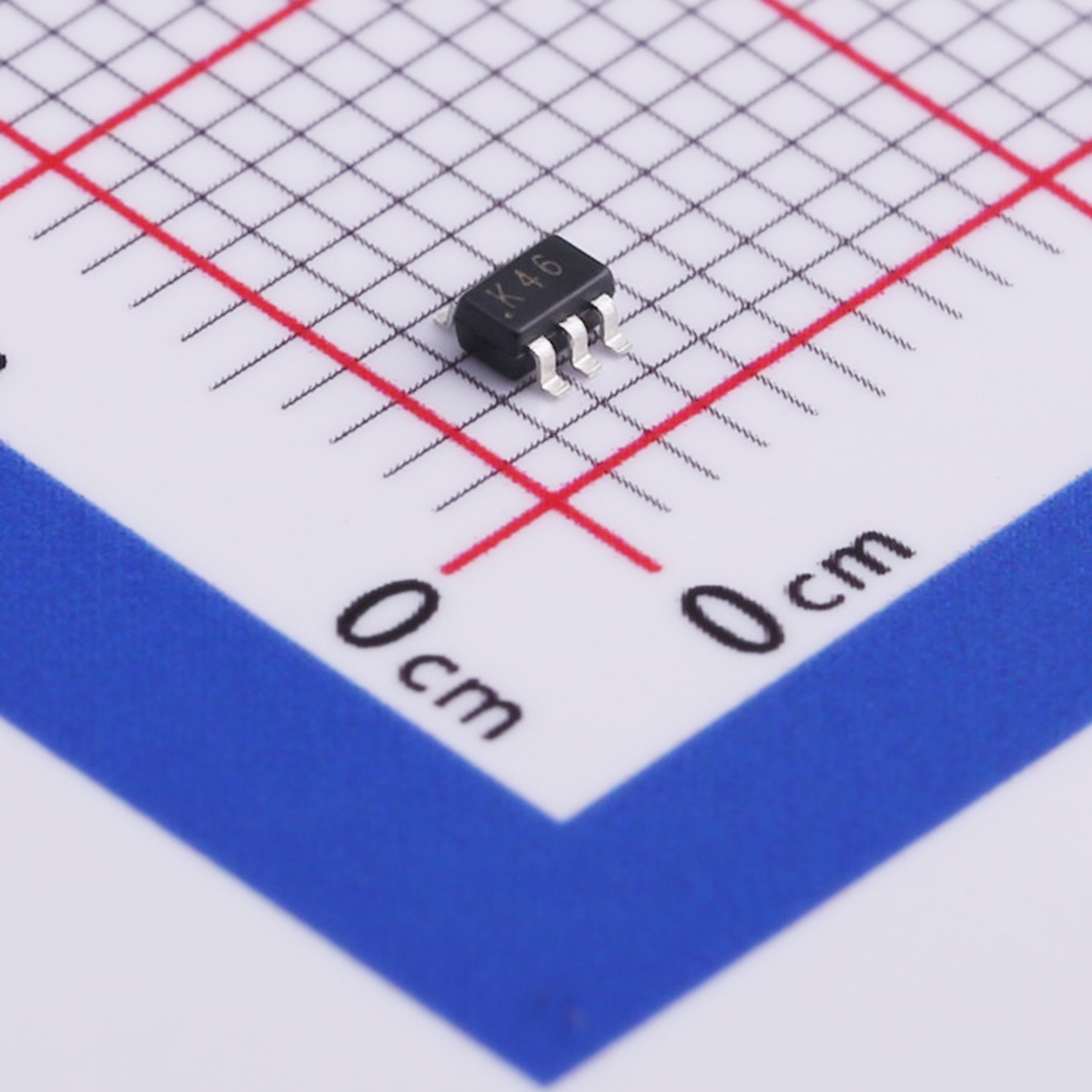
Slkor General-Purpose Signal Switching Transistor MBT3946 Product Image
1. Core Product Parameters
1.1 Maximum Ratings
- Collector-emitter voltage: 40 Vdc for NPN, -40 Vdc for PNP.
- Collector-base voltage: 60 Vdc for NPN, -40 Vdc for PNP.
- Emitter-base voltage: 6.0 Vdc for NPN, -5.0 Vdc for PNP.
- Continuous collector current: 200 mAdc for NPN, -200 mAdc for PNP.
- Total package power dissipation under 25 ℃ ambient temperature: 150 mW.
- Junction-to-ambient thermal resistance: 833 ℃/W.
- Junction and storage temperature range: -55 ℃ to +150 ℃.
1.2 Off-State Characteristics
- Collector-emitter breakdown voltage: 40 Vdc for NPN, -40 Vdc for PNP.
- Collector-base breakdown voltage: 60 Vdc for NPN, -40 Vdc for PNP.
- Emitter-base breakdown voltage: 6.0 Vdc for NPN, -5.0 Vdc for PNP.
- Maximum absolute value of base cutoff current and collector cutoff current: 50 nAdc.
1.3 On-State Characteristics
- DC current gain ranges from 100 to 300 for NPN under condition of 10 mAdc collector current and 1.0 Vdc collector-emitter voltage. For PNP, DC current gain ranges from 100 to 300 under condition of -10 mAdc collector current and -1.0 Vdc collector-emitter voltage. Gain varies under different collector-current operating conditions.
- Maximum collector-emitter saturation voltage: 0.30 Vdc for NPN, -0.40 Vdc for PNP.
- Base-emitter saturation voltage ranges: 0.65-0.95 Vdc for NPN, -0.65--0.95 Vdc for PNP.
1.4 Small-Signal Parameters
- Transition frequency: minimum 300 MHz for NPN, minimum 250 MHz for PNP.
- Output capacitance: maximum 4.0 pF for NPN, maximum 4.5 pF for PNP.
- Input capacitance: maximum 10.0 pF for NPN, maximum 8.0 pF for PNP.
- Noise figure: maximum 5.0 dB for NPN, maximum 4.0 dB for PNP.
1.5 Switching Time Parameters
- Maximum delay time and rise time: 35 ns.
- Maximum storage time: 200 ns for NPN, 225 ns for PNP.
- Maximum fall time: 75 ns for NPN, 50 ns for PNP.
1.6 Package Information
Package type: SOT-363, a compact surface-mount package. The device is mounted on FR4 glass-epoxy printed circuit board.
2. Core Product Features
- One single package integrates one NPN transistor and one PNP transistor. It eliminates the requirement for two discrete transistors, reduces PCB footprint and simplifies peripheral circuit routing for differential and push-pull circuits.
- 40 Vdc-class voltage rating and 200 mAdc collector current support both small-signal amplification and medium-low-current switch-drive operating modes.
- Wide temperature range from -55 ℃ to +150 ℃ for junction temperature, suitable for consumer-grade devices and partial industrial temperature environments.
- Satisfactory high-frequency small-signal performance. The transition frequency is no less than 300 MHz for NPN and no less than 250 MHz for PNP, which adapts to signal amplification for audio and low-radio-frequency bands.
- Well-defined switching timing parameters including delay, rise, storage and fall time, suitable for low-speed digital-signal switching-control applications.
- Controllable saturation-drop voltage with low collector-emitter voltage under turn-on status to reduce conduction power consumption. Well-defined base-emitter saturation voltage facilitates base-bias circuit design.
- Complete typical-curve references for h-parameters and noise figure. Impedance matching for audio-amplification circuits can be implemented by referring to noise characteristics varying with source resistance and operating frequency.
3. Main Application Fields
- Consumer electronic products: remote controllers, small household-appliance control boards for signal switching and audio small-signal amplification.
- Industrial-control circuit boards: low-voltage signal level conversion, small-load push-pull drive and pre-processing for sensor signals.
- Communication peripheral equipment: low-frequency signal conditioning and interface-signal buffer circuits.
- Instruments and meters: pre-amplification for weak signals and switch-drive for small loads such as relays and optocouplers.
- General analog circuits: differential amplifier circuits and complementary push-pull circuits. The on-chip NPN-PNP pair is used for constructing complementary circuits.
4. Engineering Design Recommendations
- Current and power consideration: The actual continuous collector current shall not exceed the rated value of 200 mAdc. Derate allowable power dissipation when ambient temperature rises. Evaluate junction temperature by thermal-resistance parameters and keep junction temperature below 150 ℃.
- Voltage margin design: Reserve safety margin for all inter-pole voltages. Avoid long-term operation near breakdown voltage. Reverse emitter-base voltage must not exceed the VEBO limit specified in datasheet to prevent emitter-junction damage.
- Switch-circuit design: Configure base-drive current rationally for switch applications to obtain proper saturation depth. Excessive saturation depth will increase storage time and degrade switching speed. Pay attention to timing influence introduced by delay time and storage time on overall circuits.
- Amplifier-circuit design: Select proper static collector operating current and source resistance to optimize noise performance with reference to h-parameter and noise-figure curves for small-signal-amplifier design. Input and output capacitance will affect high-frequency performance. Keep traces as short as possible for high-frequency layout to minimize superposed parasitic capacitance.
- PCB layout: Adopt the minimum recommended pad dimension for SOT-363 surface-mount package to guarantee heat dissipation and soldering reliability. Separate routing of NPN and PNP circuits to mitigate crosstalk between two channels.
- Temperature influence: DC gain and saturation voltage vary with junction temperature. Reserve circuit operating margin by reviewing typical temperature-characteristic curves for high-low-temperature operating conditions in early-stage design.
- Off-state condition: Pay attention to leakage-current specifications. For high-impedance sampling circuits, the maximum leakage current of 50 nAdc may introduce sampling error, so its circuit impact shall be evaluated.
5. Product Summary
MBT3946 is a complementary general-purpose silicon transistor housed in SOT-363 package with internal NPN and PNP devices. It features 40 Vdc withstand voltage and maximum continuous collector current of 200 mAdc. This component supports both small-signal amplification and signal-switching applications, with wide operating-temperature range and well-defined switching timing parameters. Its noise performance suits audio-signal processing. The dual-transistor-in-one-package structure simplifies design of complementary push-pull and differential circuits and saves PCB space. It is applicable to low-voltage medium-and-small-signal circuits for consumer electronics, industrial instruments and other equipment. In engineering practice, derating for voltage, current and power should be implemented. Circuit margin assessment based on temperature characteristics, switching timing and leakage-current indicators is required to achieve stable and reliable operation.
About Slkor:
SLKOR's product portfolio includes discrete semiconductor devices such as diodes, transistors, and power devices, as well as integrated circuits such as linear regulators, DC-DC converters, interface chips, Hall sensors, ADCs, and battery management systems (BMS)
MBT3946To Product Page
Related Recommendations




 粤公网安备44030002007346号