
























Service Hotline
News

News
Current status of domestic silicon carbide industry
2022-03-17
720
Study notes of a silicon carbide chip amateur. Document compilation, industry news, occasional gains, and imagination. This official account belongs to personal study notes, it is only for personal hobbies and does not involve any commercial purposes. Please forgive me if there are any irregularities in quotations in the article. Some people’s hobbies are growing flowers and grass, singing and fishing, while others like to write Twitter blogs and Douyin. In recent years, I like to occasionally read books and refresh papers on weekends to see the development of cutting-edge materials and device technologies.
Do something interesting and be an interesting soul.
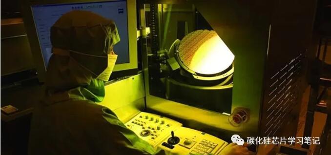
This is a topic that is easy to get scolded, but for me, who has no interests and always likes to talk nonsense, it doesn't matter if I just chat and make up the numbers. This key point is for the few people in our small circle to read by themselves. I have written it in advance to prevent myself from forgetting a few key points.
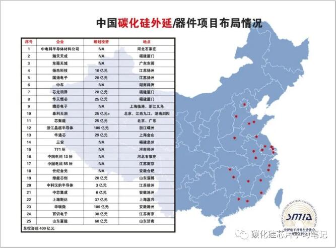
Popularity: Similar to LED back then, but the technical barriers are several orders of magnitude higher than LED;
In one sentence, we can summarize all aspects of the domestic mainstream technology direction of the industry:

1. Silica powder toner: Not a problem
The solar energy industry has done a lot of good things, and now domestic 9N silicon powder is not a big problem;
2. Silicon carbide powder: 5N is just fine, but 6N is problematic; the testing system is imperfect, and nearly two thousand furnaces are supplied on a large scale, with an annual output of millions of pieces for dozens of substrate projects. The furnaces are really turned on, and there is a huge shortage of powder! High-quality 6N silicon carbide powder sources and low-cost technical solutions priced below $100/kg are in short supply!
3. Silicon carbide crystal/wafer - 4H conductive, rare
The quality, output and cost of wafers that can be put on the truck... There is no way around it. After more than 20 years of domestic crystal growth, we have basically reached a bottleneck, which is the bottleneck of technology and money-burning iterations. The defect density/yield rate of 6-inch wafers needs to be reduced by one or two orders of magnitude. The time required for this is estimated to be 5-10 years. Let a company gather all domestic professor-level senior engineers who can grow crystals and concentrate on iterating and burning hundreds of furnaces in various improvement directions at the same time to speed up the iteration progress! The key point is that the current consumption-output ratio of this furnace is a bit melancholy if it does not make money!
Those who play capital and tell stories should not be included in this industry. It is more suitable to be in the real estate industry!
4. Silicon carbide epitaxial wafer
5-20um, N-type epitaxy, not a problem;
The backing film is not good or not enough, that is the problem!
5. Silicon carbide devices - MPS/JBS diodes
Diode - 650/1200V 20A and below, the yield is not a problem, the cost-effectiveness is reasonable; it can be stably mass-produced, and there are no big problems with the four factories in Beijing/Wuxi/Shanghai/Xiamen. The only problem is the source of good substrates that can be used in cars;
However, the yield, batch stability and overall cost of diodes of 1700V and above are still not optimistic. I have seen the actual data of several of them. The key is that sometimes the reasons for poor and unstable yields are not clear. The problem lies in the quality of the substrate and epitaxial wafer, the data does not match!
The yield rate of diodes of 50A and above is not good; but this is mostly due to the problem of the film;
6. Silicon carbide MOSFET device-planar structure
3 - 10mOhm, 20A and below. One company really has four-inch batches. The cost performance and yield/reliability need to be improved. For the time being, no company dares to install it on the car. It can be used as a charging pile for charging;
Those factories in Wuxi/Shanghai/Xiamen are all in the development and sample stages, and there is no batch data;
To sum up in one sentence: There is no planar MOSFET that can be mass-produced with stable yield and put on the market!
3mOhm 50A or more, batch stable yield exceeds 40%, no!
7. Silicon carbide MOSFET device-trench structure
——The five-year plan is under development-ing…
Completely independent patented structural products - no!
The situation of foreign MOSFET devices:
1. CREE- Only flat surfaces, no grooves; however, the performance of CREE flat structures is not worse than grooves for two to three years;
2. Japan Rohm - double groove batch shipment; there is a minor issue with the patent, which is currently being litigated; there is a minor dispute over the two-way OBC regarding reliability;
3. ST - 650V 50A specially supplied to Tesla Edamame 3, about a thousand units, the car has been running for just over a year;
4. Infenion - half pack trench;
The yield rate is unknown, but the biggest advantage of this structure is that it is stronger in the trench; but if there is a good lithography machine for 8 inches in the future, it will be a little difficult to further reduce the pitch;
To summarize in one sentence: The main mass production and shipment of foreign silicon carbide MOSFET devices is trench, which is already on the market, and the volume can be gradually increased; but I heard that the general yield rate of 6-inch MOS chips is less than 65%, and the reliability screening yield is not too optimistic! But compared to China, there is at least a five-year gap!
In terms of IP layout, it is hard to say whether there will be similar patent barriers in the silicon IGBT era in the future!
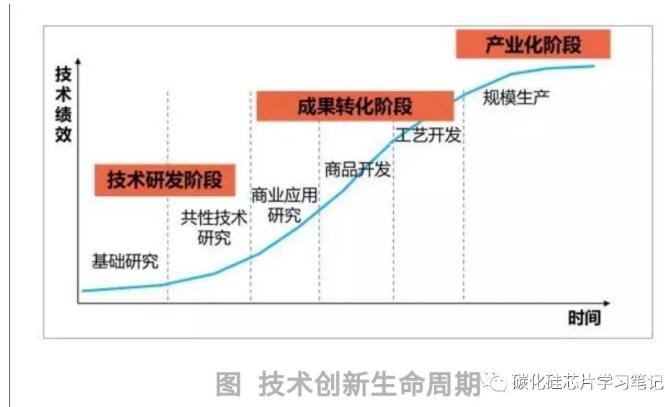
Summary of personal opinions:
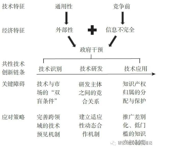
1. Crystal growth and substrate wafer are the core technologies of "stuck neck" and are common technologies in the entire industry chain. It is a bit difficult for a single market-oriented company to burn money and iterate. The company is under pressure from a profit model, and investors need good profitability statements to cash out quickly. They fully expect the company to make high investments, high risks, and burn money to improve and iterate, but there is little motivation;
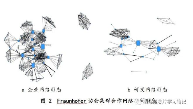
——There needs to be a non-profit research institution with national strategic investment similar to Germany's Fraunhofer Institute or Europe's IMEC to make long-term investments to solve this common technical problem!
2. Research and development of new structures for cutting-edge devices
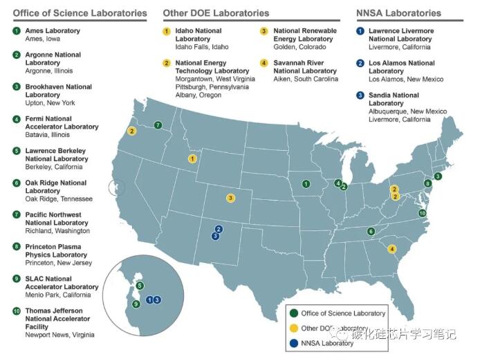
—The story of silicon IGBT cannot be repeated. Trench structure and superjunction structure need to be planned and developed in advance. There are many possible structures that are reliable and unreliable. The cost of R&D investment by enterprises alone is high. It needs an industrial joint research institution like Japan's AIST that can actually unite to invest, or a national laboratory alliance institution like Power American in the United States. Non-profit model research and development shares IP and technology authorization;
—Ga2O3, AlN, diamond and other new material systems need to be laid out in advance; companies obviously don’t have the energy to take care of it yet; we need a non-profit research investment party without conflicts of interest, China’s Fraunhofer, China’s IMEC!
Disclaimer: This article is reproduced from "Silicon Carbide Chip Study Notes". This article only represents the author's personal views and does not represent the views of Sacco Micro and the industry. It is only for reprinting and sharing to support the protection of intellectual property rights. Please indicate the original source and author for reprinting. If there is any infringement, please contact us to delete it.
Company phone number: +86-0755-83044319
Fax/FAX: +86-0755-83975897
Email: 1615456225@qq.com
QQ: 3518641314 Manager Li
QQ: 332496225 Manager Qiu
Address: Room 809, Building C, Zhantao Technology Building, No. 1079 Minzhi Avenue, Longhua New District, Shenzhen
Related Recommendations
Exclusive Interview with Li Gang of Yunfan Ruida: The Precision of Millimeter-Wave Radar Products and the Warmth of Humanity
2026-07-22
2547
RF Passion, Craftsman’s Journey: Over 30 Years of Steadfast Dedication — Interview with Kinghelm Chief Engineer Mr. Qin hongxiang
2026-06-26
2714





 粤公网安备44030002007346号