
























Service Hotline
News

News
We talk about chips every day, but do you know what a chip is?
2022-03-17
1166
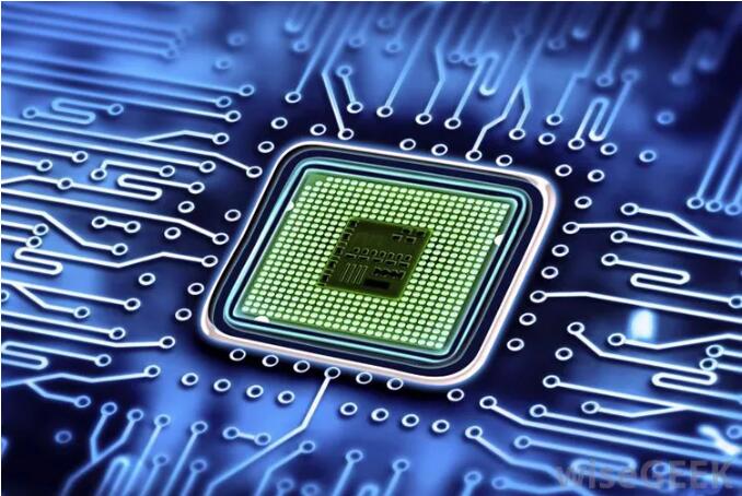
The diameter of human hair is 70,000 nanometers and the circumference is 220,000 nanometers. Manufacturing chips using a 5-nanometer process is like building 44,000 roads along a hair.
 Author: Liu Zhirong Source: Headline@Iron Tower-Liu Zhirong
On May 15, 2020, the United States issued a ban on Huawei's chips. Since then, chips have attracted widespread attention from the Chinese people. The ban came into effect on September 15. World-renowned chip manufacturers such as TSMC, MediaTek, Qualcomm, Sony, Samsung, SK Hynix, and Micron can no longer supply chips to Huawei. On September 16, the Central Commission for Discipline Inspection issued an article on its official website stating that "Huawei's chip supply cutoff may be the beginning of the nirvana of China's chip industry."
We talk about chips every day, but do you know what a chip is?
1. How has the invention of the chip changed human life??
On December 23, 1947, three scientists from Bell Labs in the United States, John Baden, William Shockley and Walter Bratton, invented the germanium crystal transistor, ushering the electronic world into the semiconductor era. The three inventors of the transistor won the 1956 Nobel Prize in Physics.
The 1950s was the golden age of semiconductors. Almost all semiconductor materials and basic processes were developed during this period.
On October 18, 1954, Texas Instruments invented the transistor radio. This radio with four transistors was small enough to fit in your pocket.
On September 12, 1958, Texas Instruments electronic engineer Jack Kilby (1923-2005) invented the integrated circuit and successfully produced the world's first integrated circuit, a chip, in 1959. This integrated circuit is to etch PNP transistors (transistors), resistors and capacitors on a germanium chip, and use external wires to connect them to form a circuit. This simple integrated circuit kicked off the chip industry, pushed human science and technology to a new peak, and completely changed the human way of life.
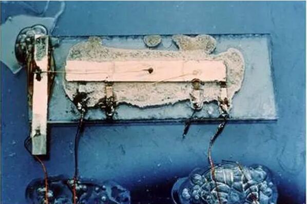
The continuous advancement of chip manufacturing technology has greatly reduced the price of a single transistor. In 1959, there were 6 transistors on a chip, equivalent to $10 per transistor; in 1971, there were 2,000 transistors on a chip, equivalent to $0.3 per transistor; in 2004, there were tens of billions of transistors on a chip, and the price of a single transistor dropped to one billionth of a dollar. The improvement in the cost performance of chips has made it possible for chips to enter ordinary people's homes.
The chip can be said to be the greatest invention of the 20th century, and many other inventions are also based on chips. Today, we live in a world surrounded by chips, and it would be difficult to move without chips.
People's daily lives are inseparable from chips. Smart devices such as mobile phones, computers, and smart watches have chips. Network equipment such as optical modems, routers, USB flash drives, memory cards, and mobile hard disks have chips. There are chips in network equipment and computer peripherals. ID cards, passports, bank cards, shopping cards, consumption cards, and other personal identification cards have chips. TVs, speakers, projectors, chargers, LED lights, electronic scales, air conditioners, refrigerators, microwave ovens, induction cookers, water heaters and other household appliances also have chips. Access control, monitoring, solar cells, etc. also need chips. If someone invented a code that disabled all the chips in the world, human life would come to a standstill.
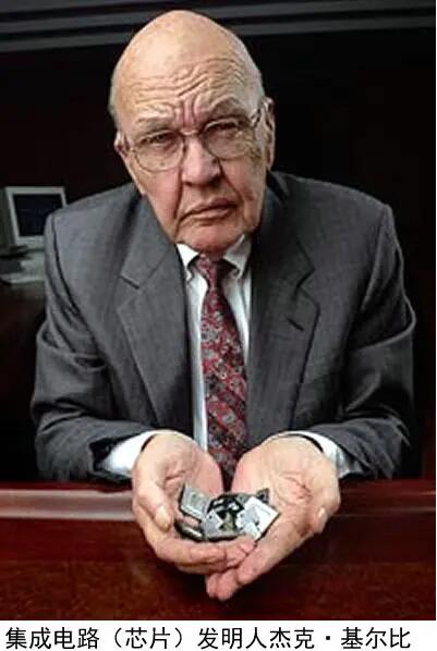 Jack Kilby won the 2000 Nobel Prize in Physics for inventing the chip. He was also the inventor of the handheld calculator and the thermal printer. When Kilby was called a scientist, he said modestly: "A scientist is a person who explains things and must have great ideas; and I am a problem solver, an engineer. My duty is to invent new processes, manufacture new products, and make money from inventions and creations."
2. To understand the chip, you must first understand the "PN junction"
As can be seen from the above, electronic components such as diodes, transistors, resistors, and capacitors are made on semiconductor materials, and then connected with wires. This is an integrated circuit, also called a chip. To understand chips, you must first understand the "PN junction", which is the core of semiconductor technology.
When a semiconductor material is doped with a pentavalent element, the electron concentration increases, forming an N-type semiconductor; when a semiconductor material is doped with a trivalent element, the hole concentration increases, forming a P-type semiconductor. "Hole" refers to the vacancy left on the covalent bond after the electrons on the covalent bond gain energy and break away from the shackles of the covalent bond to become free electrons.
After the P-type semiconductor and the N-type semiconductor are in close contact, the negatively charged electrons and positively charged holes diffuse toward each other; the diffusion of electrons and holes causes an internal electric field to form on the contact surface, and the internal electric field prevents this diffusion, allowing the electrons and holes to drift back. When the diffusion speed and drift speed of electrons and holes reach a dynamic balance, a "PN junction" is formed at the contact surface between the P-type semiconductor and the N-type semiconductor.
The main performance of "PN junction" is "single conductivity". If the P-type semiconductor end is used as the positive electrode and the N-type semiconductor end is used as the negative electrode, the current can pass through the PN junction; if the N-type semiconductor end is used as the positive electrode and the P-type semiconductor end is used as the negative electrode, the current cannot pass through the PN junction. The use of binary bits in computers is determined by the performance of the "PN junction". Current passing through the "PN junction" represents "1", and current not passing through the "PN junction" represents "0".
"PN junction" is a diode. If two P-type semiconductors sandwich an N-type semiconductor, a triode is formed, which is the PNP-type triode mentioned above. Of course, if there is a P-type semiconductor sandwiched between two N-type semiconductors, it becomes an NPN-type transistor.
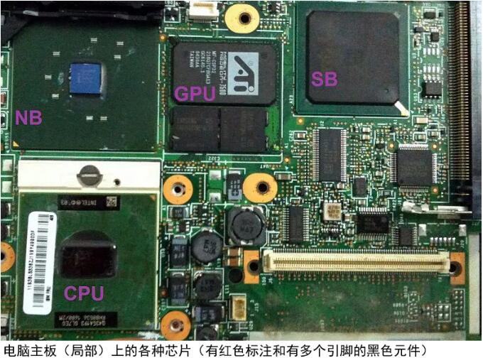
Ordinary people cannot see the "real body" of the chip. The chip is as small as a human dandruff and as large as a human fingernail. Because it is too thin, it must be packaged in a sealed shell before it can be connected to an external circuit. When you open a computer, TV or other electrical appliance, you can see a large circuit board. There are many electronic components on the circuit board. Those electronic components with multiple pins are chips. These pins are connected to the input and output terminals of the chip. Some are on both sides of the chip package, some are on four sides, and some are arranged in a matrix at the bottom, densely packed with more than 1,000 pins.
3. Making chips is like carving the earth and all road buildings on a grain of rice??
There is a concept that needs to be mentioned here, and that is "Moore's Law". In 1965, Gordon Moore, co-founder of the world-famous chip manufacturer Intel Corporation, proposed that the number of transistors on a single chip would double every year. He later corrected it to double every two years. This judgment has been verified by practice to be basically correct. In 2011, there were 2.27 billion transistors on an Intel Core i7 chip. Currently, the number of transistors on some high-end chips exceeds tens of billions. A few years ago, the AI chip WSE produced by semiconductor manufacturer Cerebras Systems using TSMC's 16nm process technology integrated 1.2 trillion transistors!
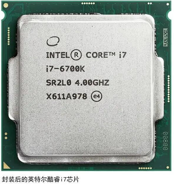
"Process" refers to the width of the transistor gate on the chip, which we can generally understand as the size of the transistor. The smaller the process, the more transistors can be made on one chip, and the larger the integrated circuit becomes.
The computing speed of chips continues to increase, thanks to the increasing integration of chips. The higher the integration level of the chip, the smaller the electronic components on it, and the shorter the wires between the electronic components. The time it takes for the current to pass through is shortened, the energy consumption is reduced, and the processing speed is accelerated.
There are three ways to make a chip carry more transistors. One is to increase the chip area, the other is to reduce the size of the transistors, and the third is to make the integrated circuit three-dimensional. Increasing the chip area is generally not considered because it will increase energy consumption and reduce the efficiency of the chip. Nowadays, people mainly take the latter two methods to increase the number of transistors on a chip.
Chip manufacturing belongs to the microscopic world, and the electronic components on it are as small as only a few atoms or molecules, and are measured in smaller units of measurement, nanometers and angstroms. The smallest scale on a general ruler is millimeters, 1 millimeter is equal to 1000 microns, 1 micron is equal to 1000 nanometers, and 1 nanometer is equal to 10 angstroms. The diameter of human hair is 70,000 nanometers and the circumference is 220,000 nanometers. Manufacturing chips using a 5-nanometer process is like building 44,000 roads along a hair.
There is a limit to reducing the size of electronic components, so people consider building multi-layer integrated circuits on one chip to increase the number of transistors. This is like building residential buildings. A single-storey house can accommodate a small number of residents, while a building with dozens of floors can accommodate a large number of residents. The stacking of integrated circuits is much more complicated than building a building. The layout of each floor of the building is the same, but the circuits of each layer of the chip are different, and the connections between layers are extremely complex.
Let’s take this metaphor a step further: manufacturing chips is like carving out a complete earth on a grain of rice, and all the roads and buildings on the earth must be carved out. Roads are the wires on the chip, and buildings are the electronic components on the chip. Through this metaphor, readers can imagine how complex and difficult it must be to manufacture chips.
4. The purification of silicon is the foundation of the chip industry
There are many semiconductor materials, but in practical applications, more than 90% of them use silicon because the melting point of silicon is 1415 degrees Celsius, which allows high-temperature processes in chip processing.
Silicon is smelted from sand, but to smelt sand into silicon that can be used to make chips requires extremely high purity. We call gold with a purity of 99.99% pure gold (4 nines), but the purity of silicon used to make chips must reach at least 11 nines, that is, there must be no more than 1 impurity atom per 1 billion silicon atoms. Silicon with this purity was refined by Bell Labs in the United States in 1955. There are currently hundreds of billions of electronic components on a chip, and the purity requirements for silicon are higher, at least 13 nines. This is the basis of chip manufacturing. Without mastering the silicon purification technology, it is impossible to create a chip!
Readers may ask, why is the silicon required to make chips so pure? The electronic components on the chip are very small. If the chip is manufactured using a 5-nanometer process, impurities of 1 nanometer will destroy the entire chip. Let us draw an analogy. If a road is 40 meters wide and there is a large stone 1 meter wide in the middle of the road, cars can avoid the stone without causing traffic jams. However, if a road is only 5 meters wide and there is a large stone 1 meter wide in the middle of the road, cars will not be able to avoid the stone, and the road will be blocked.
Therefore, manufacturing chips not only requires high purity of silicon, but also requires that all aspects of the manufacturing process be dust-free. Its purity is 100,000 times that of a hospital surgical operating room, and half of the process is even performed in a vacuum environment. Because of this, chip manufacturing plants do not need to shut down during the COVID-19 epidemic to fight the epidemic, because workers are protected from head to toe, and some protective suits even come with their own respiratory systems to prevent the chips from being contaminated by the shedding of human metabolism and exhaled gases.
5. Is the lithography machine actually an integrated circuit projector??
The name "lithography machine" is inaccurately translated and very misleading. Many people mistakenly believe that the lithography machine "carves" integrated circuits on the surface of crystalline silicon through physical contact, just like computer engraving. In fact, the chip is not "engraved" but "photographed". Therefore, it is more appropriate to call the lithography machine an "integrated circuit projector".
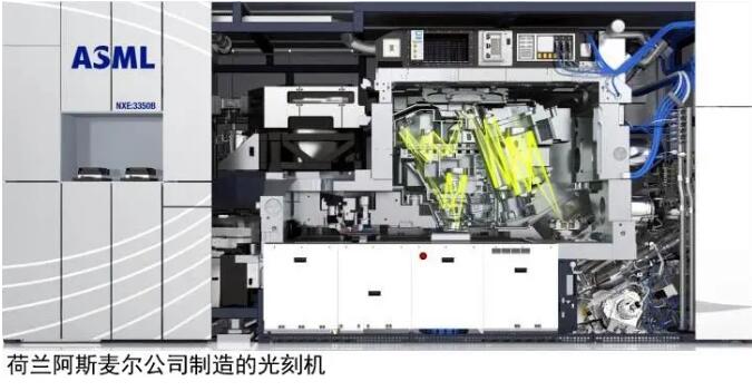
When the wafer for manufacturing the chip enters the photolithography process stage, the photolithography machine projects the integrated circuit pattern onto the photoresist on the surface of the wafer through the mask. After the photoresist is exposed, the exposed area is etched with chemical liquid and then cleaned. In this way, the integrated circuit pattern comes out. The photolithography process is the same as that of traditional photography. Light passes through the negative to sensitize the photographic paper, and then the sensitized photographic paper is developed and fixed in a chemical solution.
A chip needs to go through dozens or even hundreds of photolithography, and several processes after photolithography will take several weeks before it can enter the packaging stage.
Chip manufacturing technology is changing with each passing day, but most of the core technologies for chip manufacturing came from Bell Labs. Bell Labs’ contribution to the information technology revolution will forever go down in history.
7. Can I make chips if I have a photolithography machine? ??
Many readers are very interested in photolithography machines and think that chips can be made with photolithography machines. In fact, this is not the case. Although the photolithography machine plays an important role in chip manufacturing, it is only one of more than 1,000 processes in chip manufacturing. With the photolithography machine, if you fail to master other processes, you still cannot make a chip.
In 1961, the American GCA company manufactured the world's first photolithography machine. At present, there are 7 companies in 4 countries in the world that can manufacture lithography machines, namely Asmaier in the Netherlands, Intel, Super Technology Semiconductor, Rudolf in the United States, Nikon and Canon in Japan, and SusiMicro in Germany.
As mentioned above, the basis of the chip industry is materials, that is, the purification of silicon. Without mastering the silicon purification technology, it is impossible to produce crystalline silicon with chip-level purity, and it is impossible to make chips.
Furthermore, there are hundreds of billions of electronic components on the chip. Such a huge circuit cannot be drawn manually. Electronic design automation software EDA must be used. EDA is a comprehensive application of many natural disciplines and is monopolized by three American companies: Kadant, Synopsys and Mentor Graphics.
EDA plays a decisive role in the chip manufacturing process. The function and integration of the chip completely depend on the design capabilities of EDA. With high-purity silicon and photolithography machines, but without EDA or not knowing how to use EDA, you still can't make a chip.
Disclaimer: This article is reproduced from "IoT IQ". This article only represents the author's personal views and does not represent the views of Sacco Micro and the industry. It is only for reprinting and sharing and supports the protection of intellectual property rights. Please indicate the original source and author for reprinting. If there is any infringement, please contact us to delete it.
Company phone number: +86-0755-83044319
Fax/FAX: +86-0755-83975897
Email: 1615456225@qq.com
QQ: 3518641314 Manager Li
QQ: 332496225 Manager Qiu
Address: Room 809, Building C, Zhantao Technology Building, No. 1079 Minzhi Avenue, Longhua New District, Shenzhen
Related Recommendations
Exclusive Interview with Li Gang of Yunfan Ruida: The Precision of Millimeter-Wave Radar Products and the Warmth of Humanity
2026-07-22
2568
RF Passion, Craftsman’s Journey: Over 30 Years of Steadfast Dedication — Interview with Kinghelm Chief Engineer Mr. Qin hongxiang
2026-06-26
2735





 粤公网安备44030002007346号