
























Service Hotline
News

News
Gallium Nitride GaN or Silicon Carbide SiC?
2022-03-17
834
gallium nitridetransistors andsilicon carbideMOSFET is an emerging power semiconductor in the past two or three years. Compared with traditional silicon power semiconductors, they have many excellent characteristics: high withstand voltage, small on-resistance, small parasitic parameters, etc. They also have their own unique characteristics: the extremely small parasitic parameters and extremely fast switching speed of gallium nitride transistors make them particularly suitable for high-frequency applications. Silicon carbide MOSFET's easy drive and high reliability make it suitable for high-performance switching power supplies.
This article is based on Infineon’s gallium nitride transistor and silicon carbide MOSFET products, and provides a detailed introduction to their structures, characteristics, and application differences between the two.
As the peerless twins of the third generation of power semiconductors, gallium nitride transistors and silicon carbide MOSFETs are increasingly attracting the attention of the industry, especially electrical engineers. The reason why electrical engineers pay so much attention to these two power semiconductors is because their materials have many advantages compared with traditional silicon materials, as shown in Figure 1. The larger bandgap width and higher critical field strength of gallium nitride and silicon carbide materials make power semiconductors based on these two materials have excellent characteristics such as high withstand voltage, low on-resistance, and small parasitic parameters. When used in the field of switching power supply, it has the advantages of low loss, high operating frequency and high reliability, which can greatly improve the efficiency, power density and reliability of switching power supply.
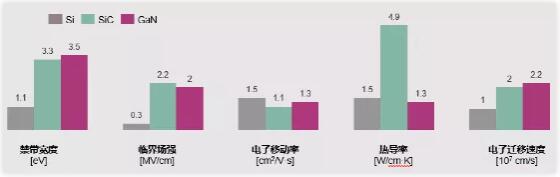 Figure 1: Comparison of key properties of silicon, silicon carbide and gallium nitride
Due to the above excellent characteristics, gallium nitride transistors and silicon carbide MOSFETs are increasingly being used in industrial fields and will be used on a larger scale. Figure 2 shows the application fields and sales forecasts of these two power semiconductors given by IHS Markit. As the application fields expand, the sales of gallium nitride transistors and silicon carbide MOSFETs will also increase significantly. Figure 3 is the sales forecast for these two power semiconductors provided by IHS Markit.
 Figure 2: Application fields and sales forecast of gallium nitride transistors and silicon carbide MOSFETs
 Figure 3: Sales forecast of gallium nitride transistors and silicon carbide MOSFETs
In Chapter 2 of this article, the structure and characteristics of gallium nitride transistors will be introduced in detail. Chapter 3 will introduce the structure and characteristics of silicon carbide MOSFET in detail. In Chapter 4, a comparative analysis will be conducted on the use of these two power semiconductors in the same circuit to more clearly explain the similarities and differences in their applications. Finally, the full text will be summarized.
Gallium nitride transistor structure and characteristics
Structure of gallium nitride transistor
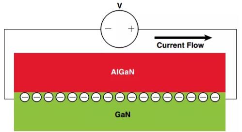 Figure 4: Schematic diagram of the conductive principle of gallium nitride
The structure of the basic gallium nitride transistor shown in Figure 4 is a depletion-mode high electron mobility transistor (HEMT), which means that when no voltage is applied between the gate and source (VGS=0V), the drain of the gallium nitride transistor and the component are conductive, that is, it is a normally-on device. This is completely different from traditional normally closed MOSFET or IGBT power switches, which are very difficult to use for industrial applications, especially in the field of switching power supplies. In order to deal with this problem, the industry usually has two solutions. One is to use a cascode structure, and the other is to add P-type gallium nitride to the gate to form an enhancement mode (normally closed) transistor. The structures of the two are shown in Figure 5.
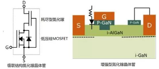 Figure 5: Two structures of gallium nitride transistors
The gallium nitride in the cascade structure is depletion-type gallium nitride cascaded with a low-voltage silicon MOSFET. The advantage of this structure is that its drive is exactly the same as that of a traditional silicon MOSFET (because it drives a silicon MOSFET). However, this structure also has great shortcomings. First, the silicon MOSFET has a body diode. When gallium nitride conducts current in the reverse direction, there is a reverse recovery problem of the body diode. Secondly, the drain of the silicon MOSFET is connected to the source of the depletion-mode gallium nitride. During the switching on and off of the silicon MOSFET, the oscillation between the drain and the source is the oscillation between the source and the gate of gallium nitride. Since this oscillation is inevitable, there is a possibility that the gallium nitride transistor may be mistakenly turned on and off. Finally, since two power devices are cascaded together, the possibility of further reducing the on-resistance of the entire gallium nitride device is limited.
Due to the above problems in the cascade structure, the mainstream technology of gallium nitride transistors in the power semiconductor industry is enhancement mode gallium nitride transistors. Taking the gallium nitride transistor CoolGaN of Infineon Technologies Co., Ltd. as an example, its detailed structure is shown in Figure 6.
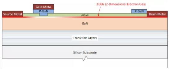 Figure 6: Schematic diagram of CoolGaN structure
As shown in Figure 6, the current gallium nitride transistor products in the industry have a planar structure, that is, the source, gate and drain are in the same plane, which is different from the vertical structure of silicon MOSFET represented by Super Junction technology. The P-GaN structure below the gate forms the enhancement mode gallium nitride transistor described earlier. Another p-GaN structure next to the drain is to solve the current collapse problem that often occurs in gallium nitride transistors. The substrate of Infineon Technologies Co., Ltd.'s CoolGaN products uses silicon material, which can greatly reduce the material cost of gallium nitride transistors. Since the thermal expansion coefficients of silicon materials and gallium nitride materials are very different, many transition layers are added between the substrate and GaN to ensure that the gallium nitride transistor will not experience failure problems such as wafer delamination under severe working conditions such as high and low temperature cycles and high and low temperature shocks.
Characteristics of gallium nitride transistors
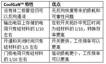 Table 1: Characteristics of CoolGaN and its advantages
From the characteristics shown in Table 1, it can be seen that gallium nitride transistors do not have a body diode but can still conduct reverse current, so they are very suitable for circuits that require reverse current flow of the power switch and will be hard-commutation, such as the totem pole bridgeless PFC in current continuous mode (CCM), which can achieve extremely high reliability and efficiency. The circuit topology diagram is shown in Figure 7. In the figure, Q1 and Q2 are gallium nitride transistors, and Q3 and Q4 are silicon MOSFETs.
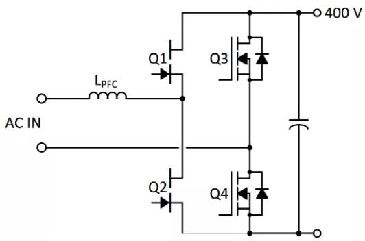 Figure 7: Schematic diagram of totem pole PFC topology using gallium nitride transistors
From Table 1, we can also know that gallium nitride has extremely fast switching speed and small driving loss, so it is very suitable for high-frequency applications. High-frequency switching power supplies using gallium nitride transistors have the advantages of high power density and high efficiency. Figure 8 shows a 3.6KW LLC topology DC-DC converter. The resonant frequency of the LLC is 350KHz. The power density of the converter reaches 160W/in^3 and the maximum efficiency exceeds 98%.
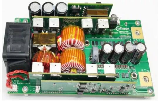 Figure 8: 3.6KW LLC conversion circuit using CoolGaN
From the above analysis, it can be seen that gallium nitride transistors are suitable for applications requiring high efficiency, high frequency, and high power density.
Silicon carbide MOSFET structure and its characteristics
Structure of silicon carbide MOSFET
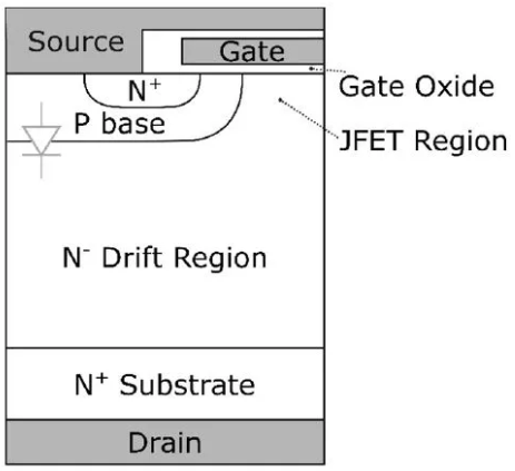 Figure 9: Schematic structural diagram of planar silicon carbide MOSFET
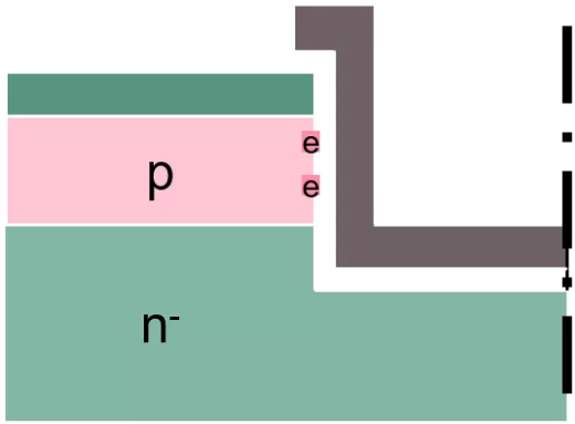 Figure 10: CoolSiC trench gate structure
Characteristics of silicon carbide MOSFET
Silicon carbide MOSFETs also have an outstanding characteristic: short circuit capability. Compared with silicon MOSFET, the short-circuit time is greatly improved, which is very important for motor drive applications such as inverters. Figure 12 shows a comparison chart of the short-circuit capabilities of CoolSiC and CoolMOS. It can be seen from the figure that CoolSiC achieves excellent characteristics such as long short-circuit time and small short-circuit current, and its reliability under short-circuit conditions is greatly improved.
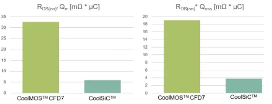 Figure 11: Performance comparison of silicon carbide MOSFET and silicon MOSFET
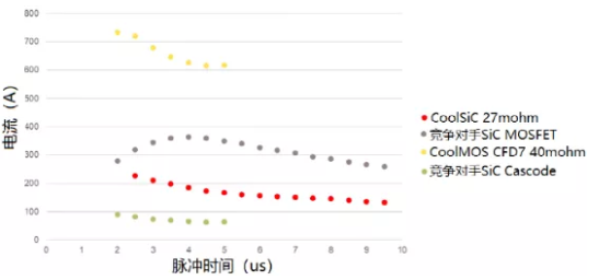 Figure 12: Comparison of short circuit capabilities of silicon carbide MOSFETs
Chapter 3 introduces the respective structures and characteristics of gallium nitride transistors and silicon carbide MOSFETs. The following will compare the parameters and actual circuits between the two.
Comparison of Gallium Nitride and Silicon Carbide MOSFETs
Electrical parameter comparison
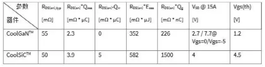 Table 2: Comparison of key parameters of CoolGaN and silicon carbide MOSFET CoolSiC
From Table 2, we can see that the dynamic parameters of gallium nitride transistors are lower than those of silicon carbide MOSFETs. Therefore, the switching losses of gallium nitride transistors are lower than those of silicon carbide MOSFETs, and their advantages will be more obvious at high operating frequencies. When the current flows in the opposite direction (source to drain), the voltage drop of the gallium nitride transistor is related to its gate-to-source drive voltage. Which one is higher and which one is lower needs to be compared according to the application situation. For the last threshold voltage Vgs(th), the value of the gallium nitride transistor is very small, which means that great attention must be paid to the drive design of the gallium nitride transistor. If the noise on the gate is large, it may cause the gallium nitride transistor to be turned on accidentally. At the same time, CoolGaN is a current-type drive mode, which is different from the traditional voltage-type drive. The threshold voltage of silicon carbide MOSFET is much higher, and its driving requirements are very close to IGBT driving.
Figure 13 shows a comparison of another important parameter, that is, the rate of change of on-resistance RDS(on) with temperature. It is well known that the on-resistance of power semiconductor switches has a positive temperature coefficient, that is, the higher the junction temperature, the greater the on-resistance. It can be seen from Figure 13 that the temperature rise coefficient of silicon carbide MOSFET is much smaller than that of silicon nitride transistor and silicon MOSFET. When the junction temperature is 100°C, the difference has reached 30% and 50%. According to Figure 13, it can be seen that assuming that the on-resistance of silicon carbide MOSFET and gallium nitride transistor is the same at a junction temperature of 25°C, in the same application circuit, it means the conduction loss of both (〖I_Drms〗^2*R_(DS(on))) The same, but when the junction temperature of the two rises to 100°C, the conduction loss of silicon carbide MOSFET is only 70% of that of silicon nitride transistor, which is very attractive for those application scenarios with harsh environmental requirements and high efficiency at high temperatures.
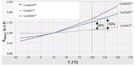 Figure 13: On-resistance curves of silicon carbide MOSFET, gallium nitride transistor and silicon MOSFET as a function of junction temperature
Application comparison
 Table 3: PFC circuit test conditions
In the test, two on-resistance devices were tested for each power switch. For the gallium nitride transistor, the RDS(on) was 35mohm and 45mohm respectively, and the silicon carbide MOSFET was 65mohm and 80mohm respectively. The test results are shown in Figure 14. Because the switching loss of the power switch is higher than the conduction loss under light load conditions, the efficiency of gallium nitride transistors is significantly higher than that of silicon carbide transistors. When the load gradually increases, the conduction loss accounts for a higher proportion of the total loss than the switching loss. At the same time, as the load increases, the temperature rise of the power switch increases. According to the change rate of the on-resistance with junction temperature in Figure 13, it can be seen that the on-resistance of the silicon carbide transistor increases less with the temperature. Therefore, the efficiency difference between the two power switches at high temperatures is very small, although the on-resistance of the silicon carbide transistor at 25°C is higher than that of the gallium nitride transistor.
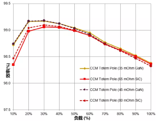 Figure 14: Silicon carbide MOSFET, gallium nitride transistor efficiency curve at PFC level
Next, we compare the calculated efficiencies of gallium nitride transistors and silicon carbide MOSFETs at different operating frequencies in a circuit topology of two-phase interleaved parallel half-bridge LLC for 3KW output power. The calculation ignores the impact of increased losses in magnetic components (including resonant inductors and main power inductors) caused by frequency increases. The circuit topology is shown in Figure 15. The model of the gallium nitride transistor selected is IGOT60R070D1 (the maximum RDS(on) at 25°C is 70mohm), with a total of 8 pcs. The silicon carbide MOSFET model selected is IMZA65R048M1H (the maximum RDS(on) at 25°C is 64mohm), a total of 8 pieces.
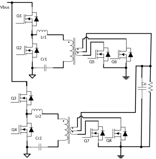 Figure 15: Schematic diagram of two-phase staggered parallel LLC circuit
Under 50% load (1500W) and normal temperature working environment, the efficiency comparison under different operating frequencies is shown in Figure 16. When the operating frequency is low (<100khz), the efficiency of using gallium nitride transistors and silicon carbide mosfets with similar on-resistance is similar, and both can achieve very high efficiency (>99.2%). When the operating frequency is increased to 300KHz , Due to its very small parasitic parameters, gallium nitride has a low proportion of switching losses in total losses, so its efficiency decreases very little (0.08%), while the efficiency of silicon carbide MOSFETs will decrease by 0.58% (99.28%-98.7%). When the operating frequency rises to 500KHz, the efficiency gap between the two becomes very large (1%). Of course, if for an actual circuit, considering that the increase in frequency will cause a sharp increase in the loss of magnetic components, the efficiency difference between the two will not be so large, but the trend of efficiency change is the same.
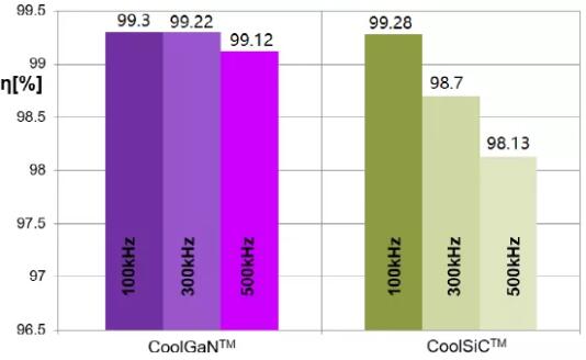 Figure 16: Efficiency comparison of two power devices at different operating frequencies
Gallium Nitride and Silicon Carbide MOSFET Application Recommendations
(1) For some reasons, the applied system must work at a frequency exceeding 200KHz. Gallium nitride transistors are the first choice, followed by silicon carbide MOSFETs. If the operating frequency is lower than 200KHz, both can be used;
(2) The applied system requires extremely high efficiency from light load to half load. Gallium nitride transistors are the first choice, followed by silicon carbide MOSFETs;
(3) If the applied system has a high maximum operating temperature, difficulty in dissipating heat, or requires extremely high efficiency at full load, silicon carbide MOSFETs are the first choice, followed by gallium nitride transistors;
(4) The applied system has large noise interference, especially gate drive interference. Silicon carbide MOSFET is the first choice, and gallium nitride transistor is the second choice;
(5) If the applied system requires a power switch with a large short-circuit capability, silicon carbide MOSFET is the first choice;
(6) For other application systems without special requirements, which product to choose depends on factors such as heat dissipation method, power density, and the designer’s familiarity with the two.
Summarize
As the industry becomes more familiar with and has more application experience, the usage of both will rise sharply, which will drive down the prices of both. This will in turn promote the wide-bandgap power semiconductors to be used on a larger scale, forming a virtuous cycle. Therefore, it is very important for electrical engineers to master and use wide bandgap power semiconductors as early as possible to improve the competitiveness of their products, improve their product visibility, and improve their own capabilities. I believe this article has great reference and reference significance for electrical engineers to become familiar with and use wide bandgap power semiconductors.
Disclaimer: This article is reprinted from "TechSugar". This article only represents the author's personal views and does not represent the views of Sacco Micro and the industry. It is only for reprinting and sharing to support the protection of intellectual property rights. Please indicate the original source and author for reprinting. If there is any infringement, please contact us to delete it.
Company phone number: +86-0755-83044319
Fax/FAX: +86-0755-83975897
Email: 1615456225@qq.com
QQ: 3518641314 Manager Li
QQ: 332496225 Manager Qiu
Address: Room 809, Building C, Zhantao Technology Building, No. 1079 Minzhi Avenue, Longhua New District, Shenzhen
Related Recommendations
Exclusive Interview with Li Gang of Yunfan Ruida: The Precision of Millimeter-Wave Radar Products and the Warmth of Humanity
2026-07-22
2585
RF Passion, Craftsman’s Journey: Over 30 Years of Steadfast Dedication — Interview with Kinghelm Chief Engineer Mr. Qin hongxiang
2026-06-26
2745





 粤公网安备44030002007346号