
























Service Hotline
News

News

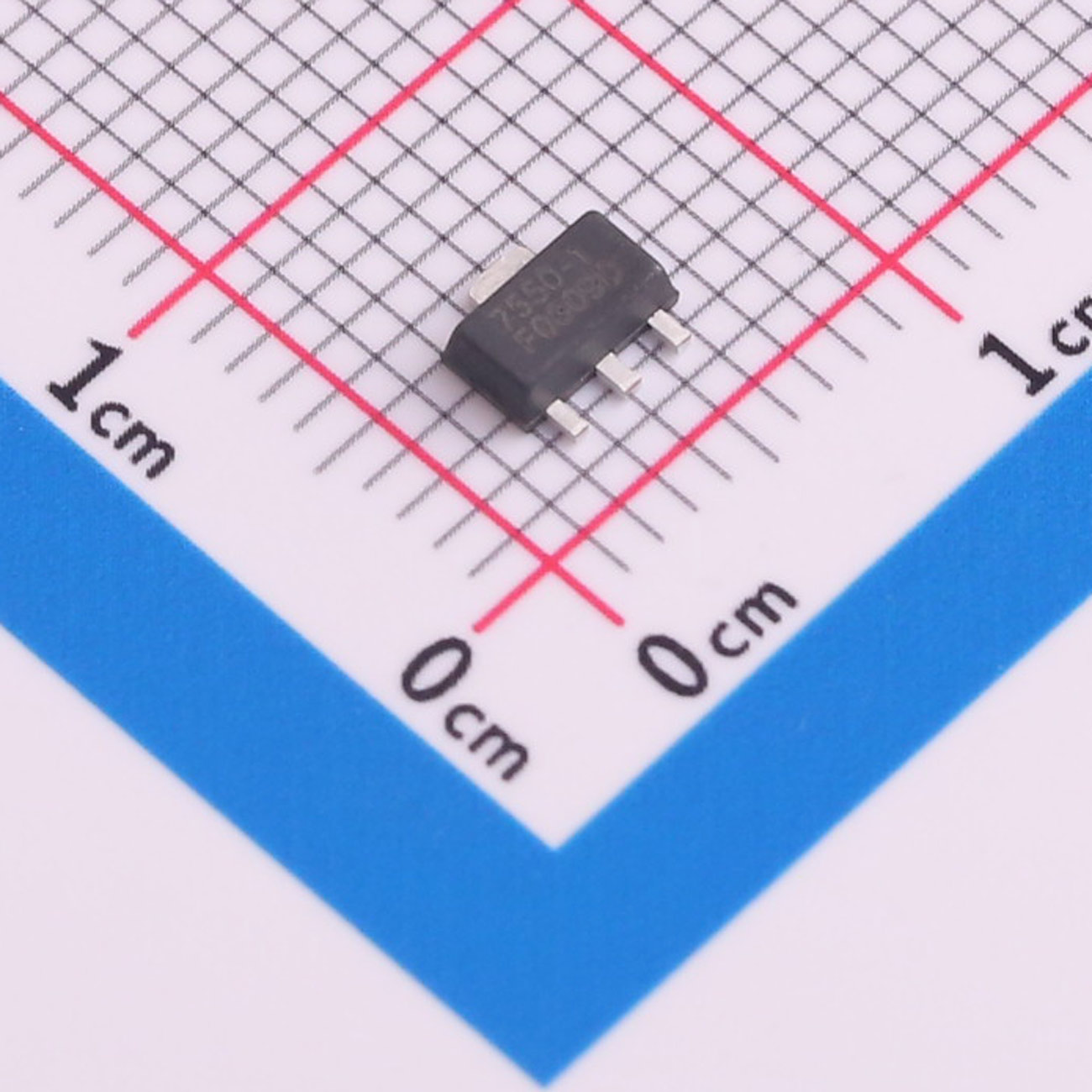
Slkor SL7550‑8 Linear Regulator: 100mA, 2.5~5V Fixed‑Output LDO Linear Regulator
2026-09-17
42
The SL75xx series are fixed-output LDO linear regulators developed by Slkor. They provide multiple fixed output voltages ranging from 2.5V to 5.0V and are available in SOT23-3, TO92 and SOT89 packages. Equipped with an internal error amplifier, the devices regulate output voltage and mitigate output drift caused by input-voltage variation and ambient-temperature fluctuation. This document sorts out device information from product parameters, core features, application fields and engineering design recommendations, offering references for hardware circuit selection and practical implementation.
About Slkor:
1. Core Product Parameters
Output Voltage Configuration
This series offers multiple fixed output voltages: 2.5V, 3.0V, 3.3V, 3.6V, 4.4V and 5.0V. The suffix "x" in part numbers denotes the package variant.
Package and Marking Information
Devices are supplied in three packages: SOT23-3, TO92 and SOT89. Corresponding device markings are 75xx-3, 75xx-9 and 75xx-8 respectively. Package types can be quickly identified by the marking.
Device Power Dissipation Calculation
Power dissipation is calculated by the formula: PD=(VIN-VOUT)×IOUT. Actual operating power dissipation must not exceed the maximum power-dissipation rating of the selected package; otherwise, device damage will occur. All parameter tests are performed under a reference ambient temperature of 25℃.
Package Dimension Specification
Complete official dimensional specifications are available for SOT23-3 and SOT89 packages. PCB design shall strictly follow the original manufacturer’s package drawings to guarantee soldering and assembly reliability.
2. Key Product Features
Voltage Regulation Principle
Built-in error amplifier compares feedback voltage Vfb obtained from resistor divider against internal reference voltage Vref, and dynamically adjusts the gate voltage of the output transistor. This suppresses output drift induced by input-voltage change and temperature variation, delivering stable fixed output voltage.
Multi-Voltage Compatibility
Covering commonly-used DC supply voltages from 2.5V to 5.0V, the multi-voltage variants satisfy power-supply requirements of various downstream chips.
Multi-Package Compatibility
Available in SOT23-3 small-size SMD, SOT89 SMD and TO92 through-hole packages. These options support compact surface-mount layout as well as manual through-hole soldering scenarios.
On-Chip Loop Compensation
Internal phase-compensation circuit works with the ESR of output capacitor to realize loop compensation, simplifying external compensation-circuit design.
3. Main Application Fields
Power Supply for Consumer-Electronic Equipment
As fixed-output LDO devices suitable for low-to-moderate-current chip power supply, SL75xx series can supply low-voltage power for MCUs, sensors and logic chips in consumer-electronic products.
Small-Scale Industrial Control Modules
They can serve as on-board auxiliary power supplies for small industrial control modules.
Power Supply for Instrument Sub-circuits
These regulators can be adopted as power components for internal sub-circuits of meters and testing equipment.
Voltage Conversion for Battery-Powered Devices
In battery-operated equipment, they convert higher battery voltage into stable fixed low voltage.
4. Engineering Design Recommendations
Output-Capacitor Selection Requirements
The internal phase compensation relies on the ESR of output capacitor. A capacitor greater than 2.2 μF must be connected from the output pin to ground to ensure stable loop operation.
Layout Guidelines for Input and Output Capacitors
10 μF polarized capacitors are recommended for both input and output terminals. Place these capacitors as close as possible to the VIN and VOUT pins of the LDO, so as to minimize adverse effects brought by lead parasitic inductance and resistance and improve transient response and anti-interference performance.
Power-Dissipation and Thermal Evaluation
Calculate real-time power dissipation using PD=(VIN-VOUT)×IOUT. The calculated value shall stay below the maximum power-dissipation rating of the selected package. When voltage drop or output current is relatively large, review package thermal parameters to prevent over-heating damage.
Device Selection and Material Verification
Check part marking during procurement and soldering to confirm output voltage and package variant and avoid incorrect component usage.
PCB Footprint Specification
Draw PCB footprints strictly in accordance with official dimensional drawings for SOT23-3, SOT89 and TO92 packages to ensure soldering reliability.
5. Product Summary
Overall Product Positioning
The SL75xx series are general-purpose fixed-output LDO linear regulators. With output-voltage coverage of 2.5V-5.0V and multiple package options, they adapt to hardware designs with different space constraints and soldering processes.
Design Constraints
Stable output is achieved via internal error-amplifier loop. Though peripheral circuits are relatively simple, clear constraints apply to capacitor selection, PCB layout, power dissipation and thermal management.
About Slkor:
SLKOR, headquartered in Shenzhen, China, is a rapidly emerging national high-tech enterprise in the power semiconductor sector. With R&D centers in Beijing and Suzhou, its core technical team originates from Tsinghua University. As an innovator in silicon carbide (SiC) power device technology, SLKOR's products are widely used in new energy vehicles, photovoltaic power generation, industrial IoT, and consumer electronics, providing critical semiconductor solutions to over 10,000 clients globally. The company delivers more than 2 billion units annually, with its SiC MOSFETs and 5th-generation ultrafast recovery SBD diodes setting industry benchmarks in efficiency ratio and thermal stability. SLKOR holds over 100 invention patents and offers 2,000+ product models, continually expanding its IP portfolio across power devices, sensors, and power management ICs. Certifications including ISO 9001, EU RoHS/REACH, and CP65 compliance demonstrate the company's steadfast commitment to technological innovation, lean manufacturing, and sustainable development.
Related Recommendations
Exclusive Interview with Li Gang of Yunfan Ruida: The Precision of Millimeter-Wave Radar Products and the Warmth of Humanity
2026-07-22
1929
RF Passion, Craftsman’s Journey: Over 30 Years of Steadfast Dedication — Interview with Kinghelm Chief Engineer Mr. Qin hongxiang
2026-06-26
2127





 粤公网安备44030002007346号