
























Service Hotline
News

News
Silicon carbide power device technical reliability materials
2022-03-16
834
Preface
The silicon carbide industry chain includes silicon carbide powder, silicon carbide ingot, silicon carbide substrate, silicon carbide epitaxy, silicon carbide wafer, silicon carbide chip and silicon carbide device packaging links. Among them, substrate, epitaxial wafer, wafer, and device packaging and testing are the four most critical links in the silicon carbide value chain. The substrate cost accounts for 50% of the total cost of silicon carbide devices, and the costs of epitaxy, wafer, and packaging testing are 25%, 20%, and 5% respectively. The reliability of silicon carbide materials is of great significance to the performance of the final device. Basic Semiconductor explores material properties and causes of defects from all aspects of the industrial chain, and collaborates with upstream and downstream companies to improve the reliability of silicon carbide power devices.

01
Silicon carbide ingot growth and preparation method
There are more than 250 isomers of silicon carbide, and the main one used to make power semiconductors is 4H-SiC single crystal structure. During the growth process of silicon carbide single crystal, the 4H crystal growth window is small, and there are strict standards for temperature and pressure design. Inaccurate control during the growth process will result in silicon carbide crystals with other structures such as 2H, 3C, 6H and 15R.
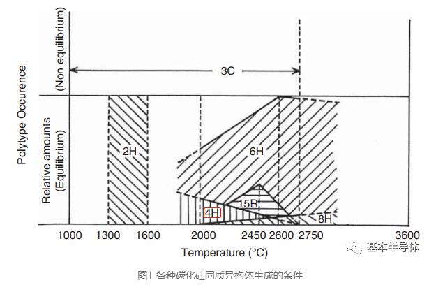
Figure 1 Conditions for the generation of various silicon carbide isomers
In the industry, there are three methods for preparing silicon carbide single crystal ingots: sublimation PVT, HT-CVD, and LPE (solution growth method). Among them, sublimation PVT is currently the most mainstream preparation method. About 95% of commercial silicon carbide ingots are grown from PVT. The process is to put silicon carbide powder into special equipment and heat it. After the temperature rises to 2200-2500°C, the powder begins to sublimate. Since silicon carbide has no liquid state, only gaseous and solid states, an ingot will crystallize on the top after sublimation. The growth rate of silicon single crystal is about 300mm/h, and the growth rate of silicon carbide single crystal is about 400μm/h. The difference between the two is nearly 800 times. For example, the formation of a five- to six-centimeter ingot requires continuous and stable growth for 200-300 hours. It can be seen that the preparation rate of silicon carbide ingots is very slow, which makes the ingots expensive.
02
Silicon carbide single crystal ingot and substrate wafer defects
Both silicon carbide ingots and substrate wafers contain a variety of crystal defects, such as stacking faults, microtubules, through screw dislocations, through edge dislocations, basal plane dislocations, etc. Defects in silicon carbide ingots will greatly affect the yield of the final device. This is a very important topic in the industry chain. All substrate manufacturers are sparing no effort to reduce the defect density of silicon carbide ingots.
03
Silicon carbide substrate reliability
The substrate sheet is a product obtained by cutting the crystal ingot into thin slices, smoothing and polishing it. The substrate wafer obtains good surface quality after the polishing process, which can suppress the generation of defects during epitaxial growth, thereby obtaining high-quality epitaxial wafers. Its surface quality includes flatness, near-surface dislocations and residual stress. In order to suppress the generation of defects during the initial stages of epitaxial growth, the substrate surface must be stress-free and free of near-surface dislocations. If the residual damage near the surface is not sufficiently removed, epitaxial growth on the substrate will lead to the generation of macroscopic defects. Therefore, the quality level of the substrate link will seriously affect the quality level of the subsequent epitaxial growth link.
04
Silicon carbide epitaxial growth and reliability
Epitaxy refers to growing a layer of single crystal material 4H-SiC that is homogeneous with the substrate on the upper surface of the substrate. Silicon carbide has many isomers. In order to ensure the preparation of high-quality epitaxial materials, special technology is required to avoid the introduction of other crystal forms. The current standardized process is to use 4° bevel-cut 4H-SiC single crystal substrates and adopt step controlled growth technology. The commonly used process at present is the CVD method: the commonly used equipment is a hot wall horizontal epitaxial furnace, and the commonly used reaction precursor gas is silane (SiH4), methane (CH4), ethylene (C2H4), etc., and use nitrogen (N2) and trimethylaluminum (TMA) as impurity sources. The typical growth temperature range is 1500~1650 ℃, and the growth rate is 5~30μm/h.
The growth of the epitaxial layer can eliminate many surface or near-surface defects introduced during crystal growth and wafer processing, so that the crystal lattice is arranged neatly and the surface morphology is greatly improved compared to the substrate. Thick epitaxial layer, good surface morphology and lower doping concentration are important for improving breakdown voltage. Such epitaxial wafers are used to manufacture power devices, which can greatly improve parameter stability and yield.
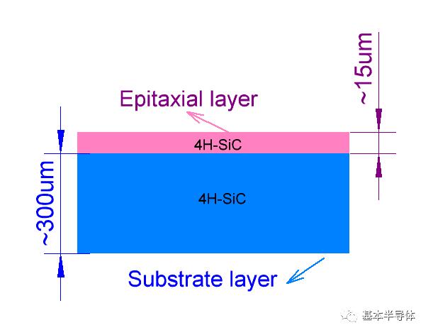
Figure 2 Structure of substrate layer and epitaxial layer
05
The relationship between defects in silicon carbide epitaxial wafers and substrate wafers
As mentioned above, defects in the silicon carbide epitaxial layer are related to the substrate and the growth process. Epitaxial layer defects include surface topography defects, micropipe defects, dislocations and other types. Surface morphology defects include carrot defects (comet-type in some cases), shallow pits, triangular defects, and dropped objects; microtubule defects in the substrate will be copied to the epitaxial layer. The current density of microtubules in the substrate is far below 0.1/cm2, basically eliminated. Most of the dislocations in the silicon carbide epitaxial layer originate from substrate dislocations, which mainly include TSD, TED and BPD. Defects introduced by epitaxy such as ordinary dislocations and carrot defects are important issues affecting the quality of silicon carbide epitaxy.
06
The impact of silicon carbide epitaxial wafer defects on the final device
During the epitaxial growth process, about 98% of TSD in the substrate is converted into TSD, and the rest is converted into Frank SFs; TED is 100% converted into TED; about 95% of BPD is converted into TED, and a small amount is maintained as BPD.
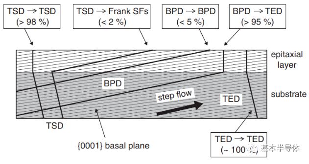
Figure 3 Correlation between silicon carbide epitaxial wafer defects and substrate wafer defects
TSD and TED basically do not affect the performance of the final silicon carbide device, while BPD can cause degradation of device performance, so people pay more attention to BPD. Stacking faults, carrot defects, triangle defects, dropped objects and other defects are killer defects. Once they appear on a device, the device will fail the test, resulting in a reduction in yield. Bipolar devices, such as triodes and IGBTs, are more sensitive to BPD.
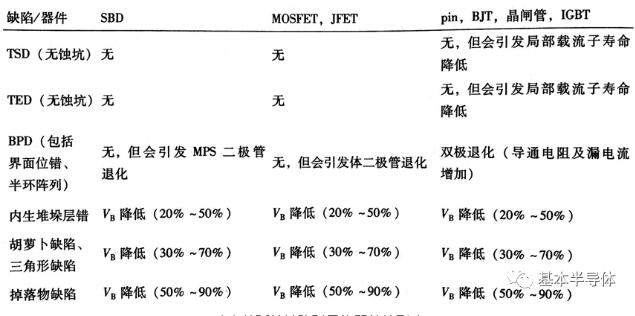
Table 1 The impact of epitaxial wafer defects on the final device
07
Two challenges facing silicon carbide materials
One of the important challenges facing the promotion of silicon carbide materials is that the price is too high, and the substrate price is much higher than that of silicon and sapphire substrates. At present, the mainstream diameter of silicon carbide substrate is only 4 to 6 inches, and more mature growth technology is needed to expand the size and reduce the price.
On the other hand, the dislocation density of silicon carbide is on the order of 102-104, which is much higher than that of silicon, gallium arsenide and other materials. In addition, silicon carbide also has large stress, which can cause problems with surface parameters. Improving the quality of silicon carbide substrates is an important way to improve the quality of epitaxial materials, device preparation yield, device reliability and lifespan.
Disclaimer: This article is reprinted from "Basic Semiconductor", which supports the protection of intellectual property rights. Please indicate the original source and author of the reprint. If there is any infringement, please contact us to delete it.
Company phone number: +86-0755-83044319
Fax/FAX: +86-0755-83975897
Email: 1615456225@qq.com
QQ: 3518641314 Manager Li
QQ: 332496225 Manager Qiu
Address: Room 809, Building C, Zhantao Technology Building, No. 1079 Minzhi Avenue, Longhua New District, Shenzhen
Related Recommendations
Exclusive Interview with Li Gang of Yunfan Ruida: The Precision of Millimeter-Wave Radar Products and the Warmth of Humanity
2026-07-22
2503
RF Passion, Craftsman’s Journey: Over 30 Years of Steadfast Dedication — Interview with Kinghelm Chief Engineer Mr. Qin hongxiang
2026-06-26
2675





 粤公网安备44030002007346号