
























Service Hotline
News

News
Application direction of silicon carbide Schottky diodes! Guojing Micro Semiconductor
2022-03-16
1061
This article mainly introduces the application fields and development history of silicon carbide diodes, and explains in detail the classification and structure of silicon carbide MOS tubes. The only component of silicon and carbon is silicon carbide (SiC), commonly known as emery. Silicon carbide occurs in nature as the mineral moissanite, but is very rare. However, powdered silicon carbide has been produced in large quantities as an abrasive since 1893. Silicon carbide has been used as an abrasive for over a hundred years, primarily in grinding wheels and many other abrasive applications.
“SiC has a high resistance until the threshold voltage (VT) is reached. When the threshold voltage is reached, its resistance will decrease significantly until the applied voltage drops below VT. The earliest electrical applications of SiC that took advantage of this property were lightning arresters in power distribution systems (shown in the figure).
Since SiC has a varistor, the SiC stem can be connected between high-voltage lines and ground. If a power line is struck by lightning, the power supply voltage will rise and exceed the threshold voltage (VT) of the SiC arrester, thereby directing and delivering the lightning current to the ground (instead of the power line), thereby causing no harm. But these SiC arresters conduct too much current at the normal operating voltage of the power line. Therefore, the spark gaps must be connected in series. When the voltage on the power line rises due to a lightning strike, the spark gap will ionize and conduct electricity, effectively connecting the SiC arrester between the power line and the ground. Later, relevant personnel discovered that the spark gap used by the arrester was unreliable. Due to material failure, dust or salt intrusion, it may happen that the spark gap fails to trigger the arc when needed or fails to extinguish the arc after a lightning strike. Silicon carbide arresters were originally designed to eliminate the dependence on spark gaps, but due to their reliability, gapped silicon carbide arresters have mostly been replaced by zinc oxide core gapless varistors.
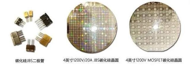
There are many types of semiconductor devices produced from silicon carbide, including Schottky diodes (also called Schottky barrier diodes or SBDs), J-type field-effect transistors (or JFETs), and field-effect transistors used in high-power switching applications. Some companies have begun to try to apply silicon carbide Schottky diode bare chips to power electronic modules. In fact, silicon substrates have been widely used in IGBT power modules and power factor correction circuits.
One of the reasons silicon carbide-based power electronic components are so attractive is that at a given blocking voltage, their doping density is almost a hundred times higher than that of silicon-based devices. In this way, a high blocking voltage with low on-resistance can be obtained. Low on-resistance is important for high-power applications because when on-resistance is reduced, less heat is generated, reducing the thermal load on the system and increasing overall efficiency.
However, there are some difficulties in the production of silicon carbide-based electronic components, and the elimination of defects has become the most important issue. These defects will result in poor reverse barrier properties of components made from SiC crystals. In addition to crystal quality issues, interface issues between silicon dioxide and SiC also hinder the development of SiC-based power MOSFETs and insulated gate bipolar crystals. Fortunately, using nitriding technology in production can greatly reduce the defects that cause these interface problems.
Silicon carbide is still used as an abrasive in many industrial applications. It is mainly used as a polishing film in the electronics industry to polish both ends of optical fibers before splicing. These can bring a high degree of smoothness to fiber optic connectors for efficient operation. Silicon carbide has been produced for over a hundred years but has only recently been used in the power electronics industry. Due to its special physical and electrical properties, it is very useful in high pressure and high temperature applications.
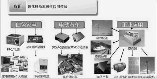
Today, silicon carbide diodes are used in various fields.
1. Solar inverter.
Silicon carbide diodes are the basic material of solar power diodes and are superior to ordinary bipolar diode technology in various technical indicators. Silicon carbide diodes switch very quickly on and off and have no reverse recovery current when switching using normal bipolar diode technology. After eliminating the reverse recovery current effect, silicon carbide diodes reduce energy consumption by 70% and can maintain high energy efficiency over a wide temperature range, thus increasing the flexibility of designers to optimize system operating frequency.
2. New energy vehicle charger.
After passing automotive product testing, the breakdown voltage of silicon carbide diodes has been increased to 650 volts, which can meet the requirements of designers and car manufacturers to reduce the voltage compensation coefficient, thereby ensuring a sufficient safety margin between the nominal voltage and the instantaneous peak voltage of on-board rechargeable semiconductor components. The dual-tube diode product maximizes space utilization and reduces the weight of the car charger.
First. Classification of SiC devices.
Silicon carbide metal oxide semiconductor field effect transistor.
Silicon carbide field effect transistors are the most concerned devices in the research of silicon carbide power electronic devices. Nowadays, silicon materials are approaching the theoretical performance limit, and silicon carbide power devices are regarded as "ideal devices" because of their high withstand voltage, low loss and high efficiency. However, compared with previous silicon devices, the balance between performance and cost and the need for high technology will be the key to promote the development of silicon carbide power devices.
Second, the structure of silicon carbide MOS.
The N+ source region and metal oxide semiconductor field effect transistor are N+ doped by ion implantation and annealed at 1700°C. Another key process is the formation of silicon carbide metal oxide semiconductor gate oxide. Because both silicon and carbon atoms are present in silicon carbide, a very specific method of growing the gate dielectric is required. The advantages of the groove structure are as follows:
The trench structure of silicon carbide field effect transistors can give full play to the characteristics of silicon carbide.
Third, the advantages of silicon carbide MOS.
Generally speaking, silicon IGBTs can only operate at frequencies below 20kHz. Due to material limitations, high-voltage and high-frequency silicon devices cannot be realized. Silicon carbide MOSFETs are not only suitable for a wide voltage range from 600V to 10kV, but also have the excellent switching performance of unipolar devices. Compared with silicon IGBTs, silicon carbide field effect transistors have lower switching losses and higher operating frequencies when there is no current tail in the switching circuit.
The loss of a 20kHz silicon carbide MOSFET module can be half that of a 3kHz silicon IGBT module, and a 50A silicon carbide module can replace a 150A silicon module. It shows the huge advantages of silicon carbide metal oxide semiconductor field effect transistors in terms of operating frequency and efficiency.
The parasitic body diode reverse recovery time trr and reverse recovery charge Qrr of silicon carbide MOSFET are very small. As shown in the figure, the reverse charge of the parasitic diode of a silicon carbide MOSFET is only 5% of the reverse charge of a silicon-based MOSFET with the same voltage specification. For bridge circuits (especially when the LLC converter operates above the resonant frequency), this indicator is critical to reduce losses and noise caused by dead time and body diode reverse recovery, and helps improve the switching frequency.
Fourth, the application of silicon carbide MOS tubes!
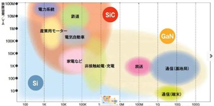
Silicon carbide MOSFET modules have great advantages in applications in medium and high power systems such as photovoltaic power generation, wind power generation, electric vehicles and rail transit. The advantages of high voltage, high frequency and high efficiency of silicon carbide devices can break through the limitations of device performance in existing electric vehicle designs, which is the focus of research and development in the field of electric vehicles at home and abroad. foreign. For example, the power control units (PCU) in hybrid electric vehicles (HEV) and pure electric vehicles (EV) jointly developed by Denso and Toyota use silicon carbide MOSFET modules, thereby reducing the volume ratio to 1/5. The EV motor drive system developed by Mitsubishi uses SiCMOSFET modules to integrate the power drive module into the motor, thereby achieving the goals of integration and miniaturization. It is expected that silicon carbide MOSFET modules will be widely used in electric vehicles at home and abroad in recent years.
Wuxi Guojing Micro Semiconductor Technology Co., Ltd. is a high-tech innovative enterprise dedicated to the research, development and industrialization of silicon carbide SiC power devices, gallium nitride GaN optoelectronic devices and conventional integrated circuits. It works on silicon carbide field effect transistors. Design, production and sales of silicon carbide Schottky diodes, GaN optocoupler relays, single-chip integrated circuits and other product chips, and provide supporting services for related product overall solution design. The headquarters is located in Wuxi High-tech Development Zone, Jiangsu Province, and has R&D centers, sales service support centers and offices in Shenzhen and Hong Kong.
The company's silicon carbide power devices cover 650V/2A-100A, 1200V/2A-90A, 1700V/5A-80A and other series. The products have been put into mass production, and the products are completely comparable to the advanced quality and level of international brands. It has successively launched full-current, full-voltage silicon carbide Schottky diodes and silicon carbide MOSFET series products, and has passed industrial-grade and automotive-grade reliability tests, and its performance has reached the international advanced level. They are used in solar inverter power supplies, new energy electric vehicles and charging piles. , smart grid, high-frequency welding, rail transportation, industrial control special power supply, national defense and military industry and other fields. Due to its high-speed switching and low on-resistance characteristics, it can exhibit excellent electrical characteristics even under high-temperature conditions, greatly reducing switching losses, making components smaller, lighter, and more efficient, and improving the reliability of the entire system, which can improve system reliability. The maximum power range of electric vehicles can be reduced by 10%, the weight of the entire vehicle can be reduced by about 5%, and safe and stable operation can be achieved in the high-temperature environment of the charging pile where it is designed to be used.
Most of the engineers in the company's core R&D team have a master's degree or above, and many PhDs are responsible for the development of the project. The company has established a standardized system for scientific and technological innovation and intellectual property management. It has accumulated many core technologies in circuit design, semiconductor device and process design, reliability design, device model extraction, etc., and has multiple international and domestic independent invention patents.
“SiC has a high resistance until the threshold voltage (VT) is reached. When the threshold voltage is reached, its resistance will decrease significantly until the applied voltage drops below VT. The earliest electrical applications of SiC that took advantage of this property were lightning arresters in power distribution systems (shown in the figure).
Since SiC has a varistor, the SiC stem can be connected between high-voltage lines and ground. If a power line is struck by lightning, the power supply voltage will rise and exceed the threshold voltage (VT) of the SiC arrester, thereby directing and delivering the lightning current to the ground (instead of the power line), thereby causing no harm. But these SiC arresters conduct too much current at the normal operating voltage of the power line. Therefore, the spark gaps must be connected in series. When the voltage on the power line rises due to a lightning strike, the spark gap will ionize and conduct electricity, effectively connecting the SiC arrester between the power line and the ground. Later, relevant personnel discovered that the spark gap used by the arrester was unreliable. Due to material failure, dust or salt intrusion, it may happen that the spark gap fails to trigger the arc when needed or fails to extinguish the arc after a lightning strike. Silicon carbide arresters were originally designed to eliminate the dependence on spark gaps, but due to their reliability, gapped silicon carbide arresters have mostly been replaced by zinc oxide core gapless varistors.
SiC in power electronics
There are many types of semiconductor devices produced from silicon carbide, including Schottky diodes (also called Schottky barrier diodes or SBDs), J-type field-effect transistors (or JFETs), and field-effect transistors used in high-power switching applications. Some companies have begun to try to apply silicon carbide Schottky diode bare chips to power electronic modules. In fact, silicon substrates have been widely used in IGBT power modules and power factor correction circuits.
Advantages and Disadvantages of SiC
One of the reasons silicon carbide-based power electronic components are so attractive is that at a given blocking voltage, their doping density is almost a hundred times higher than that of silicon-based devices. In this way, a high blocking voltage with low on-resistance can be obtained. Low on-resistance is important for high-power applications because when on-resistance is reduced, less heat is generated, reducing the thermal load on the system and increasing overall efficiency.
However, there are some difficulties in the production of silicon carbide-based electronic components, and the elimination of defects has become the most important issue. These defects will result in poor reverse barrier properties of components made from SiC crystals. In addition to crystal quality issues, interface issues between silicon dioxide and SiC also hinder the development of SiC-based power MOSFETs and insulated gate bipolar crystals. Fortunately, using nitriding technology in production can greatly reduce the defects that cause these interface problems.
SiC abrasive disc
Silicon carbide is still used as an abrasive in many industrial applications. It is mainly used as a polishing film in the electronics industry to polish both ends of optical fibers before splicing. These can bring a high degree of smoothness to fiber optic connectors for efficient operation. Silicon carbide has been produced for over a hundred years but has only recently been used in the power electronics industry. Due to its special physical and electrical properties, it is very useful in high pressure and high temperature applications.
Today, silicon carbide diodes are used in various fields.
1. Solar inverter.
Silicon carbide diodes are the basic material of solar power diodes and are superior to ordinary bipolar diode technology in various technical indicators. Silicon carbide diodes switch very quickly on and off and have no reverse recovery current when switching using normal bipolar diode technology. After eliminating the reverse recovery current effect, silicon carbide diodes reduce energy consumption by 70% and can maintain high energy efficiency over a wide temperature range, thus increasing the flexibility of designers to optimize system operating frequency.
2. New energy vehicle charger.
After passing automotive product testing, the breakdown voltage of silicon carbide diodes has been increased to 650 volts, which can meet the requirements of designers and car manufacturers to reduce the voltage compensation coefficient, thereby ensuring a sufficient safety margin between the nominal voltage and the instantaneous peak voltage of on-board rechargeable semiconductor components. The dual-tube diode product maximizes space utilization and reduces the weight of the car charger.
3. Advantages of switching power supply.
The use of silicon carbide switches very quickly, can operate at high frequencies, and has zero recovery and temperature-independent properties. Utilizing our low inductance RP packages, these diodes can be used in any number of fast switching diode circuits or high frequency converters.
4. Industrial advantages.
Silicon carbide diodes: Mainly used in high-frequency power converters in heavy-duty motors and industrial equipment, bringing the advantages of high efficiency, high power and high frequency.
SiC devices
First. Classification of SiC devices.
Silicon carbide metal oxide semiconductor field effect transistor.
Silicon carbide field effect transistors are the most concerned devices in the research of silicon carbide power electronic devices. Nowadays, silicon materials are approaching the theoretical performance limit, and silicon carbide power devices are regarded as "ideal devices" because of their high withstand voltage, low loss and high efficiency. However, compared with previous silicon devices, the balance between performance and cost and the need for high technology will be the key to promote the development of silicon carbide power devices.
Second, the structure of silicon carbide MOS.
The N+ source region and metal oxide semiconductor field effect transistor are N+ doped by ion implantation and annealed at 1700°C. Another key process is the formation of silicon carbide metal oxide semiconductor gate oxide. Because both silicon and carbon atoms are present in silicon carbide, a very specific method of growing the gate dielectric is required. The advantages of the groove structure are as follows:
The trench structure of silicon carbide field effect transistors can give full play to the characteristics of silicon carbide.
Third, the advantages of silicon carbide MOS.
Generally speaking, silicon IGBTs can only operate at frequencies below 20kHz. Due to material limitations, high-voltage and high-frequency silicon devices cannot be realized. Silicon carbide MOSFETs are not only suitable for a wide voltage range from 600V to 10kV, but also have the excellent switching performance of unipolar devices. Compared with silicon IGBTs, silicon carbide field effect transistors have lower switching losses and higher operating frequencies when there is no current tail in the switching circuit.
The loss of a 20kHz silicon carbide MOSFET module can be half that of a 3kHz silicon IGBT module, and a 50A silicon carbide module can replace a 150A silicon module. It shows the huge advantages of silicon carbide metal oxide semiconductor field effect transistors in terms of operating frequency and efficiency.
The parasitic body diode reverse recovery time trr and reverse recovery charge Qrr of silicon carbide MOSFET are very small. As shown in the figure, the reverse charge of the parasitic diode of a silicon carbide MOSFET is only 5% of the reverse charge of a silicon-based MOSFET with the same voltage specification. For bridge circuits (especially when the LLC converter operates above the resonant frequency), this indicator is critical to reduce losses and noise caused by dead time and body diode reverse recovery, and helps improve the switching frequency.
Fourth, the application of silicon carbide MOS tubes!
Silicon carbide MOSFET modules have great advantages in applications in medium and high power systems such as photovoltaic power generation, wind power generation, electric vehicles and rail transit. The advantages of high voltage, high frequency and high efficiency of silicon carbide devices can break through the limitations of device performance in existing electric vehicle designs, which is the focus of research and development in the field of electric vehicles at home and abroad. foreign. For example, the power control units (PCU) in hybrid electric vehicles (HEV) and pure electric vehicles (EV) jointly developed by Denso and Toyota use silicon carbide MOSFET modules, thereby reducing the volume ratio to 1/5. The EV motor drive system developed by Mitsubishi uses SiCMOSFET modules to integrate the power drive module into the motor, thereby achieving the goals of integration and miniaturization. It is expected that silicon carbide MOSFET modules will be widely used in electric vehicles at home and abroad in recent years.
Wuxi Guojing Micro Semiconductor Technology Co., Ltd. is a high-tech innovative enterprise dedicated to the research, development and industrialization of silicon carbide SiC power devices, gallium nitride GaN optoelectronic devices and conventional integrated circuits. It works on silicon carbide field effect transistors. Design, production and sales of silicon carbide Schottky diodes, GaN optocoupler relays, single-chip integrated circuits and other product chips, and provide supporting services for related product overall solution design. The headquarters is located in Wuxi High-tech Development Zone, Jiangsu Province, and has R&D centers, sales service support centers and offices in Shenzhen and Hong Kong.
The company's silicon carbide power devices cover 650V/2A-100A, 1200V/2A-90A, 1700V/5A-80A and other series. The products have been put into mass production, and the products are completely comparable to the advanced quality and level of international brands. It has successively launched full-current, full-voltage silicon carbide Schottky diodes and silicon carbide MOSFET series products, and has passed industrial-grade and automotive-grade reliability tests, and its performance has reached the international advanced level. They are used in solar inverter power supplies, new energy electric vehicles and charging piles. , smart grid, high-frequency welding, rail transportation, industrial control special power supply, national defense and military industry and other fields. Due to its high-speed switching and low on-resistance characteristics, it can exhibit excellent electrical characteristics even under high-temperature conditions, greatly reducing switching losses, making components smaller, lighter, and more efficient, and improving the reliability of the entire system, which can improve system reliability. The maximum power range of electric vehicles can be reduced by 10%, the weight of the entire vehicle can be reduced by about 5%, and safe and stable operation can be achieved in the high-temperature environment of the charging pile where it is designed to be used.
Most of the engineers in the company's core R&D team have a master's degree or above, and many PhDs are responsible for the development of the project. The company has established a standardized system for scientific and technological innovation and intellectual property management. It has accumulated many core technologies in circuit design, semiconductor device and process design, reliability design, device model extraction, etc., and has multiple international and domestic independent invention patents.
"The country's most important weapon, starting from crystallization, self-improvement, self-reliance, and achieving century-old success" is the common goal of Guojing Micro Semiconductor. We provide excellent development space for our employees and provide high-quality products and services to our customers. We sincerely look forward to a win-win future with you. .
Disclaimer: This article is reproduced from "Network" and supports the protection of intellectual property rights. If there is any infringement, please contact us to delete it.
Company phone number: +86-0755-83044319
Fax/FAX: +86-0755-83975897
Email: 1615456225@qq.com
QQ: 3518641314 Manager Li
QQ: 332496225 Manager Qiu
Address: Room 809, Building C, Zhantao Technology Building, No. 1079 Minzhi Avenue, Longhua New District, Shenzhen
Related Recommendations
Exclusive Interview with Li Gang of Yunfan Ruida: The Precision of Millimeter-Wave Radar Products and the Warmth of Humanity
2026-07-22
2518
RF Passion, Craftsman’s Journey: Over 30 Years of Steadfast Dedication — Interview with Kinghelm Chief Engineer Mr. Qin hongxiang
2026-06-26
2688





 粤公网安备44030002007346号