
























Service Hotline
News

News
The “problem” of eight-inch fabs
2022-03-17
947
To be conservative, the current supply chain situation for 8-inch (200mm) wafers is quite severe!
However, this is by no means a new problem. TrendForce, a market research company in Taiwan, released a news release in November 2020 saying: "In terms of 8-inch wafer production capacity, there has been a serious supply shortage problem since the second half of 2019."
In addition, to make matters worse, a fire broke out at the Renesas Electronics Naka factory in March 2021. The problem is exacerbated by the fact that Renesas's factory here supplies many models.
Based on the above background, many factors are "entangled" together. However, it goes without saying that the biggest reason is COVID-19. Due to the COVID-19 epidemic, the demand for various electronic products such as headphones, computers, TVs, display screens, and mobile phones has surged.
Although cars also fall into the above categories, people still hope that the car market will recover from the shadow of the new crown epidemic in 2021. Nowadays, various products are promoting the SoC (System on Chip) model that integrates multiple functions into one. Therefore, many products need to be equipped with multiple ICs with digital-analog mixed signal (Mixed Signal Chip). The main uses of the above products are as follows: PMIC (Power Management IC), CMOS image sensor, fingerprint recognition sensor, automobile engine/chassis control, display driver IC, Sub Giga Hertz wireless communication chip, etc. Under normal circumstances, the above are suitable for 180nm and 350nm processes and are produced on 8-inch wafers.
That is, the growing demand for products used in this type of mixed signal chip (Mixed Signal Chip) and power semiconductors has led to insufficient production capacity of 8-inch wafers.
Affected by the supply limit of 8-inch wafers, the foundry is likely to expand its production capacity. The foundry may acquire the 8-inch wafer production equipment and production lines of the vertical integrated manufacturer (IDM: Integrated Device Manufacturer). Examples that can be cited are as follows: Recent reports indicate that UMC in Taiwan is discussing the acquisition of the 8-inch production line of Japan Semiconductor (formerly Toshiba's semiconductor manufacturing company).
No manufacturer provided
As Trend Force’s report pointed out, the reason for the severe semiconductor supply shortage that began in the second half of 2019 is that almost no manufacturers can produce 8-inch wafer equipment, even now, so the price of semiconductor production equipment continues to rise.
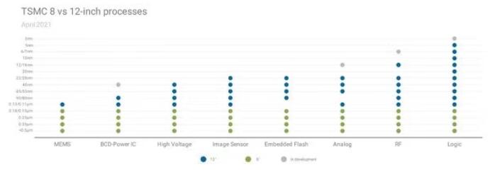
In other words, as far as the situation of 8-inch wafers is concerned, it is better to say that it is characterized by "insufficient supply manufacturers" rather than "supply chain chaos". Part of the 12-inch wafer is "moved"
As for 12-inch (300mm) wafer foundries, various companies represented by TSMC and GLOBALFOUNDRIES are investing enthusiastically to expand production capacity. However, no improvements can be seen for 8-inch.
Since there has been no improvement in 8-inch wafer production capacity, some manufacturers are switching from existing 180nm and 350nm 8-inch production lines to 12-inch wafers. In addition, many foundries can provide 130nm processes produced on 12-inch wafers, so they can be used as secondary or primary supply sources. Therefore, this helps improve the geographical diversity of the supply chain. Characteristics of 180nm and 130nm process technology
Although the 180nm and 130nm processes have similar processes, they also have differences. The main reason is that the threshold voltage of the transistor drops to different degrees. The core supply voltage is 1.8V to 1.5V, or as low as 1.2V. In addition, there are various process technology options to support 5V/3.3V IO voltages, and these process characteristics are very similar for passive components that are extremely important for analog/RF design.
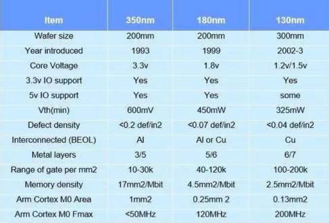
Comparison chart of major node technologies used in Mixed Signal ASIC and other products. (Picture from: eetimes)
12-inch wafer technology has several advantages. Since copper can be used instead of aluminum in older generation technologies, the allowable current density is also higher and the electromigration resistance is also excellent. In addition, there are more metal layers and the transistor size is smaller. Therefore, by increasing the transistor density and wiring density, the chip size can be reduced and performance improved.In addition, most 180nm process technologies and most 130nm BCD (Bipolar-CMOS-DMOS) process technologies can support functions such as STI (Shallow Trench Isolation). Therefore, compared with the LOCOS (Local Oxidation of Silicon) insulation used in most 350nm technologies, higher density, latch up protection functions, etc. can be obtained. Therefore, the effect of improving line performance and stability is achieved.
Today, the 130nm BCD process is quite mature and therefore can be used as an option for various process technologies. Such as different levels of high-voltage transistors, non-volatile storage semiconductors, MIM (metal-insulating film-metal) capacitors, Zener diodes/Schottky diodes, etc. Therefore, not only can complex analog/RF functions be integrated with SoC solutions, but other benefits can also be provided. 8-inch wafers also have many advantages
8-inch wafers also have many advantages. For example, the price advantage of 8-inch wafers manufactured at 350 nanometers.
The reasons are as follows: the production equipment has been depreciated and the production process is relatively simple (fewer layers). In addition, some analog circuits may not be able to be successfully miniaturized in the new process, so the price of a semiconductor chip of the same level as 130 nm may be higher than that of 350 nm. However, when a product cannot be produced due to a shortage of parts, in most cases an extremely serious situation occurs, rather than a simple cost difference in semiconductor chips.
In addition, people’s focus at this stage is that although various foundries are switching from 8 inches to 12 inches, no one manufacturer has made any statement. Although manufacturers skilled in Mixed Signal ASIC are working hard, they should first start with the ports of the circuit diagram and the data sheet of the IC.
In terms of the investment required to redesign the ASIC, other products should be coordinated to avoid the same problems as the 8-inch supply chain.
The 130nm feature size is smaller, so it can be integrated with the "Arm Cortex-M" series cores without increasing cost. The chip area required for low-end CPU is only a few square millimeters, and it is possible to integrate it with 64kbit/128kbit SRAM with high efficiency.
Judging from today's data sheet, the schedule from designing ASIC, mass production, and obtaining certification takes 14 months to 24 months (depending on the complexity). The initial Proto Type Silicon should be completed within a year. If it is an automotive product, it takes about 24 months to 36 months (depending on the complexity) from the production of specifications to PPAP (Production part approval process, production part approval process). The general budget for a 130nm ASIC starts at US$600,000 (depending on the actual complexity and IP content). If based on AEC-Q100, the cost is about US$4 million. Today, the cost of Mask Tool for the 130nm process (12-inch wafer) is less than US$200,000, accounting for a low proportion of the overall cost.
Many Mixed Signal Devices are manufactured from 8-inch wafers that are in short supply. Due to insufficient investment in 8-inch wafer production lines (due to low investment returns), supply chain problems will continue to exist in the future.
This shortage of semiconductor supply is a "warning" to some extent. Companies currently using 8-inch wafers should first consider future demand. In addition, whether it is the main production base or the second supplier (Second Source), sufficient time needs to be ensured before all processes are completed.
Disclaimer: This article is reproduced from "Semiconductor Industry Observation". This article only represents the author's personal views and does not represent the views of Sacco Micro and the industry. It is only for reprinting and sharing to support the protection of intellectual property rights. Please indicate the original source and author for reprinting. If there is any infringement, please contact us to delete it.
Company phone number: +86-0755-83044319
Fax/FAX: +86-0755-83975897
Email: 1615456225@qq.com
QQ: 3518641314 Manager Li
QQ: 332496225 Manager Qiu
Address: Room 809, Building C, Zhantao Technology Building, No. 1079 Minzhi Avenue, Longhua New District, Shenzhen
Related Recommendations
Exclusive Interview with Li Gang of Yunfan Ruida: The Precision of Millimeter-Wave Radar Products and the Warmth of Humanity
2026-07-22
2533
RF Passion, Craftsman’s Journey: Over 30 Years of Steadfast Dedication — Interview with Kinghelm Chief Engineer Mr. Qin hongxiang
2026-06-26
2696





 粤公网安备44030002007346号