
























Service Hotline
News

News
Enjoy power surfing! ST masterGaN? platform opens the era of smaller, lighter and faster gallium nitride charging
2022-03-17
768
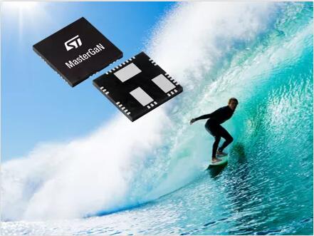
Beyond Moore’s Law, third-generation semiconductor material technology reaches its peak moment
Since the beginning of the 21st century, the rise of new applications such as artificial intelligence, 5G, and autonomous driving has put forward higher requirements for chip performance. It has also promoted continuous innovation in semiconductor manufacturing processes and new materials. As the third generation of semiconductor material technologies that may surpass Moore's Law, they have ushered in their highlight moment.
The third generation semiconductor materials, also known as Wide Bandgap Semiconductors, are those semiconductor materials with a large bandgap width (Eg≥2.3 eV). The mainstream silicon carbide (SiC) and gallium nitride (GaN), as well as the non-mainstream zinc oxide (ZnO), diamond and aluminum nitride (AlN) are the main representatives of the third generation semiconductor technology. Compared with the first and second generation semiconductor materials, in addition to a wider energy gap, the third generation semiconductors also have excellent breakdown field strength, thermal conductivity, electron saturation rate and radiation resistance. They have advantages in manufacturing high-temperature, high-frequency, radiation-resistant and high-power devices, and can meet the urgent need for more energy-efficient energy conversion systems. According to Omdia's "2020 SiC and GaN Power Semiconductor Report", global sales revenue of SiC and GaN power semiconductors is expected to reach US$854 million by the end of 2020. It will achieve double-digit annual growth rates over the next ten years and will exceed US$5 billion by 2029.
Many new applications such as electric vehicles, 5G, and big data have brought development opportunities to semiconductor materials. In applications such as power-hungry data centers, various chargers, and traction motor inverters for electric vehicles that are about to replace internal combustion engines, improvements in energy efficiency will reduce the carbon dioxide produced by traditional energy consumption such as oil and coal. New materials also promote the large-scale application of renewable energy. For example, wide bandgap power semiconductors can make solar and wind power generation more efficient.
On the other hand, with the deployment and application of the Internet of Things (IoT) based on 5G, the Internet of Everything becomes popular on a large scale, and billions of users, machines and devices can share large amounts of data, high-resolution images and high-definition video streams in real time. Remote surgery, self-driving cars, drone delivery and many other challenging applications will become a reality from concept to reality. In addition to benefiting from artificial intelligence (AI) and machine learning, these developments are also inseparable from new materials with higher processing performance, higher bandwidth and short latency.
In the early 1990s, ST has been developing and launching SiC MOSFET transistors and diodes starting from 2-inch wafers. After years of long-term investment, ST has obtained key patents for related core manufacturing processes. Whether it is epitaxial layers, edge termination design, or gate oxide layers, ST's high-voltage transistor and diode manufacturing expertise has played an important role in helping ST take the lead in successfully developing SiC. nowST has leveraged this momentum to become a key SiC supplier in the emerging electric vehicle (EV) industry. ST's SiC products are mainly used in on-board charging of electric vehicles, main inverters, DC-DC converters, industrial drives, photovoltaics and other applications. At the same time, ST remains committed to developing GaN devices for applications such as 5G base stations and communication towers, power switches, consumer electronics and industrial chargers and power adapters. GaN-on-silicon RF products are currently being designed, which will enable ST to maximize its product portfolio.
In terms of SiC MOSFET, ST is establishing a stable supply chain: the successful acquisition of Sweden's Norstel AB completed a complete vertical supply chain integration, signed long-term wafer supply agreements with Cree and SiCrystal, and also continued to expand its own production capacity. now,ST is building on its SiC successContinue to GaN field, actively carrying out a series of cooperation with the upstream and downstream of the industry chain: acquiring a majority stake in gallium nitride innovator Exagan, adopting TSMC's industry-leading GaN manufacturing process, cooperating with Leti to develop silicon-based gallium nitride power conversion technology, working with MACOM to increase silicon-based GaN production capacity, etc. The launch of ST masterGaN® platform: opening up the era of smaller, lighter and faster GaN charging
The trend of power supply miniaturization has been going on for decades and is expected to continue to enable new market applications. In addition, increasing power density is the key to improving energy efficiency and is also a parameter that designers attach great importance to. However, there are still major technical limitations in how to achieve more compact and efficient power solutions.
As a new wave of innovation, GaN high electron mobility transistor technology is revolutionizing the world of power engineering. GaN power FET transistors break through the performance limitations of ordinary silicon-based power solutions, enabling high speed, high efficiency and higher power density that silicon-based MOSFETs have never achieved, and empowering new application markets. As a leader and pioneer in the power conversion market for decades, ST leverages its unparalleled technical experience and system expertise to ride this new wave of innovation and continuously launch new products and solutions to cover a wider range of market applications.
Recently, ST launched the world's first product platform masterGaN® that integrates a silicon-based half-bridge driver chip and a pair of GaN transistors. This integrated solution will help accelerate the development of the next generation of lightweight, energy-saving chargers and power adapters below 400W for consumer electronics and industrial applications.
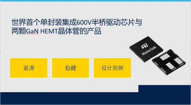
GaN technology enables electronic devices to processMore power, while the device itself becomesSmaller, lighter and more energy efficient, these improvements will transform ultra-fast chargers and wireless chargers for smartphones, USB-PD compact adapters for PCs and game consoles, as well as industrial applications such as solar power storage systems, uninterruptible power supplies, or high-end OLED TVs and cloud servers.
In today's GaN market, discrete power transistors and driver ICs are often used, which requires designers to learn how to make them work together to achieve optimal performance. STMicroelectronics’ masterGaN solution bypasses this challenge, shortening time to market and achieving expected performance while making the package smaller and simpler, with fewer circuit components and higher system reliability. Leveraging the advantages of GaN technology and STMicroelectronics’ integrated products, chargers and adapters using the new products are more efficient than conventional silicon-based solutions.Reduce size by 80%, reduce weight by 70%, and increase charging speed by 2 times。
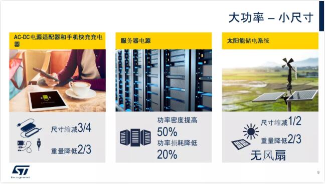
The unique advantages of masterGaN product platform
Matteo Lo Presti, executive vice president and general manager of the Analog Products Division of STMicroelectronics, said: "ST's unique masterGaN product platform is based on our market-proven expertise and design capabilities, integrating high-voltage smart power BCD process and GaN technology, which can accelerate the development of space-saving, energy-efficient and environmentally friendly products."
masterGaN1 is the first product of STMicroelectronics’ masterGaN platform, integrating two half-bridge configuration GaN power transistors and high- and low-side driver chips. masterGaN1 is packaged in a 9mm x 9mm GQFN package with a thickness of only 1mm and is now in mass production. In addition, STMicroelectronics also provides a product evaluation board to help customers quickly start power product projects.
Disclaimer: This article is reprinted from "STMicroelectronics China". This article only represents the author's personal views and does not represent the views of Sacco Micro and the industry. It is only for reprinting and sharing to support the protection of intellectual property rights. Please indicate the original source and author for reprinting. If there is any infringement, please contact us to delete it.
Company phone number: +86-0755-83044319
Fax/FAX: +86-0755-83975897
Email: 1615456225@qq.com
QQ: 3518641314 Manager Li
QQ: 332496225 Manager Qiu
Address: Room 809, Building C, Zhantao Technology Building, No. 1079 Minzhi Avenue, Longhua New District, Shenzhen
Related Recommendations
Exclusive Interview with Li Gang of Yunfan Ruida: The Precision of Millimeter-Wave Radar Products and the Warmth of Humanity
2026-07-22
2568
RF Passion, Craftsman’s Journey: Over 30 Years of Steadfast Dedication — Interview with Kinghelm Chief Engineer Mr. Qin hongxiang
2026-06-26
2735





 粤公网安备44030002007346号