
























Service Hotline
News

News
Popular Science: The Origin of Semiconductors
2022-03-16
1942
Semiconductors, we are currently discussing a lot about materials, devices, investment, etc. Each topic has a different focus. The materials are nothing more than third-generation wide-bandgap semiconductor materials; the devices are mainly MOS, HEML, etc. based on WBG materials, which we have talked about before; I won’t go into details about investment, industry trends, corporate information, stock market, etc. Today we are going to talk about the history of the semiconductor industry and learn about the origins of the semiconductor industry.
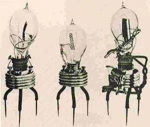
It has two major functions: switching and amplification. Switching refers to turning on and off current, and amplification refers to amplifying current or small signals while maintaining the original characteristic functions of the signal. However, there are a series of disadvantages, such as large size, easy connection loosening, short lifespan and rapid aging.
This series of shortcomings led to its inevitable development or replacement. In 1949, John Bardeen, Walter Brattin, and William of Bell Labs The Shockleys (William Shockley) invented the electronic amplifier made of the semiconductor material germanium, which was the first generation transistor (these three scientists won the 1956 Nobel Prize in Physics). The transistor was originally called a "transmission resistor" and was later renamed a transistor.
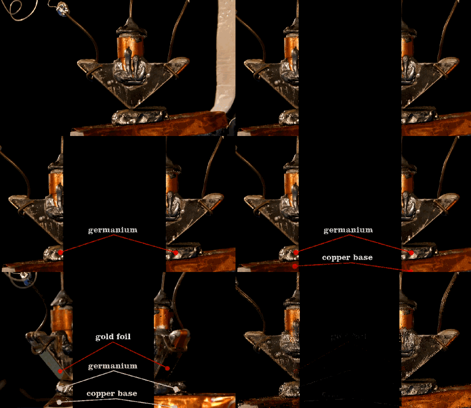
This kind of transistor includes the functions of a vacuum tube, and is solid-state, has no vacuum, has the advantages of small size, light weight, low power consumption and long life. Since then, we have entered the "solid-state era", which is what we have seen the most so far.
The development from the first transistor to many of our current power electronic devices has led to a rapid development of power electronics technology. These devices are generally referred to as discrete devices, that is, each chip contains only one component. Another semiconductor-related device that we have not mentioned before is integrated circuits.
The first integrated circuit was invented by Jack Kilby of Texas Instruments, but it was not the form of today's integrated circuit.
It was initially connected by separate wires, but earlier Jean Horni of Fairchild Camera had developed a planar manufacturing process that formed electronic junctions on the chip surface to make transistors, taking advantage of silicon's ease of forming insulator silicon oxide. Robert Noyce then applied this technology to connect discrete devices preformed on the silicon surface, eventually forming the pattern used by all integrated circuits.
Process improvement: Manufacturing devices and circuits in smaller sizes, allowing them to have higher density, greater quantities, and higher reliability.
Structural improvements: Inventions in new device designs enable better performance, better energy consumption control and higher reliability.
The effects brought about by these two improvements can be well understood from the development history of several generations of IGBT. Of course, many of the factors we mentioned before, such as some defects in the equipment process, etc., can be attributed to process improvements.
The size and number of devices in integrated circuits are two common signs of IC development. The size of the device is expressed by the smallest size in the design, which we call the feature pattern size. The development from small-scale integrated circuits to today's million chips has benefited from the reduction of the feature pattern size of a single component, which has benefited from the great improvement of photolithography machine patterning process and multi-layer wiring technology. This is also discussed a lot nowadays, such as 22nm chips, 10nm or even 7nm, etc. A more professional expression is gate width, that is, we control the width of part of the gate. Smaller and faster transistors and higher-density circuits benefit from smaller gate widths. Speaking of this, I have to mention the term "Moore's Law" that I often saw some time ago. Gordon Moore, one of the founders of Intel, predicted in 1965 that the number of transistors on a chip would double every 18 months. After years of actual verification, this rate is relatively accurate and has become the basis for predicting the density of transistors on chips in the future. According to the number of devices in the circuit, that is, the level of integration, we can divide it into several levels: small-scale integration (SSI): 2~50 units/chip; medium-scale integration (MSI): 50~5000 units/chip; large-scale integration (L SI): 5000~100000 pieces/chip; Very Large Scale Integration (VLSI): 100000~1000000 pieces/chip; Very Large Scale Integration (ULSI): >1000000 pieces/chip.
Moore's Law does not develop without limit over time. It is mainly limited by the limitations of semiconductor materials and preparation. Therefore, we will hear the news that the semiconductor material silicon is approaching its limit. Therefore, it is necessary to develop new materials and continuously improve equipment and design.
Manufacturing a rectangular chip on a circular wafer results in some unusable area remaining at the edge of the wafer. When the chip size is larger, these unusable areas will also be larger, so larger-sized wafers are gradually adopted, which "reduces" the size of the chip in disguise, and also improves production efficiency and output. This is one of the reasons why the wafer has changed from 6 inches to 8 inches and now to 12 inches.
Today's chip sizes are getting smaller and smaller, costs are getting lower and lower, and performance is getting higher and higher. This is due to the process improvements and equipment development we mentioned above, which has also led to increasingly fierce competition in the semiconductor industry.
For now, there are roughly three types of manufacturers: integrated device manufacturers (IDM): integrating design, manufacturing, packaging and sales; Foundry: other chip suppliers manufacture chips; Fabless: only responsible for chip design and sales, and most other links are outsourced. Of course, there are other interleaved models. At the same time, the localization of semiconductors has led to more and more domestic semiconductor manufacturers and more and more enterprise models.
Vacuum triodes "provoke trouble"
It has two major functions: switching and amplification. Switching refers to turning on and off current, and amplification refers to amplifying current or small signals while maintaining the original characteristic functions of the signal. However, there are a series of disadvantages, such as large size, easy connection loosening, short lifespan and rapid aging.
This series of shortcomings led to its inevitable development or replacement. In 1949, John Bardeen, Walter Brattin, and William of Bell Labs The Shockleys (William Shockley) invented the electronic amplifier made of the semiconductor material germanium, which was the first generation transistor (these three scientists won the 1956 Nobel Prize in Physics). The transistor was originally called a "transmission resistor" and was later renamed a transistor.
This kind of transistor includes the functions of a vacuum tube, and is solid-state, has no vacuum, has the advantages of small size, light weight, low power consumption and long life. Since then, we have entered the "solid-state era", which is what we have seen the most so far.
The development from the first transistor to many of our current power electronic devices has led to a rapid development of power electronics technology. These devices are generally referred to as discrete devices, that is, each chip contains only one component. Another semiconductor-related device that we have not mentioned before is integrated circuits.
integrated circuit
The first integrated circuit was invented by Jack Kilby of Texas Instruments, but it was not the form of today's integrated circuit.
It was initially connected by separate wires, but earlier Jean Horni of Fairchild Camera had developed a planar manufacturing process that formed electronic junctions on the chip surface to make transistors, taking advantage of silicon's ease of forming insulator silicon oxide. Robert Noyce then applied this technology to connect discrete devices preformed on the silicon surface, eventually forming the pattern used by all integrated circuits.
Craftsmanship and Trends
Process improvement: Manufacturing devices and circuits in smaller sizes, allowing them to have higher density, greater quantities, and higher reliability.
Structural improvements: Inventions in new device designs enable better performance, better energy consumption control and higher reliability.
The effects brought about by these two improvements can be well understood from the development history of several generations of IGBT. Of course, many of the factors we mentioned before, such as some defects in the equipment process, etc., can be attributed to process improvements.
The size and number of devices in integrated circuits are two common signs of IC development. The size of the device is expressed by the smallest size in the design, which we call the feature pattern size. The development from small-scale integrated circuits to today's million chips has benefited from the reduction of the feature pattern size of a single component, which has benefited from the great improvement of photolithography machine patterning process and multi-layer wiring technology. This is also discussed a lot nowadays, such as 22nm chips, 10nm or even 7nm, etc. A more professional expression is gate width, that is, we control the width of part of the gate. Smaller and faster transistors and higher-density circuits benefit from smaller gate widths. Speaking of this, I have to mention the term "Moore's Law" that I often saw some time ago. Gordon Moore, one of the founders of Intel, predicted in 1965 that the number of transistors on a chip would double every 18 months. After years of actual verification, this rate is relatively accurate and has become the basis for predicting the density of transistors on chips in the future. According to the number of devices in the circuit, that is, the level of integration, we can divide it into several levels: small-scale integration (SSI): 2~50 units/chip; medium-scale integration (MSI): 50~5000 units/chip; large-scale integration (L SI): 5000~100000 pieces/chip; Very Large Scale Integration (VLSI): 100000~1000000 pieces/chip; Very Large Scale Integration (ULSI): >1000000 pieces/chip.
Moore's Law does not develop without limit over time. It is mainly limited by the limitations of semiconductor materials and preparation. Therefore, we will hear the news that the semiconductor material silicon is approaching its limit. Therefore, it is necessary to develop new materials and continuously improve equipment and design.
Chip and wafer size
Manufacturing a rectangular chip on a circular wafer results in some unusable area remaining at the edge of the wafer. When the chip size is larger, these unusable areas will also be larger, so larger-sized wafers are gradually adopted, which "reduces" the size of the chip in disguise, and also improves production efficiency and output. This is one of the reasons why the wafer has changed from 6 inches to 8 inches and now to 12 inches.
Today's chip sizes are getting smaller and smaller, costs are getting lower and lower, and performance is getting higher and higher. This is due to the process improvements and equipment development we mentioned above, which has also led to increasingly fierce competition in the semiconductor industry.
For now, there are roughly three types of manufacturers: integrated device manufacturers (IDM): integrating design, manufacturing, packaging and sales; Foundry: other chip suppliers manufacture chips; Fabless: only responsible for chip design and sales, and most other links are outsourced. Of course, there are other interleaved models. At the same time, the localization of semiconductors has led to more and more domestic semiconductor manufacturers and more and more enterprise models.
write at the end
Related Recommendations
Exclusive Interview with Li Gang of Yunfan Ruida: The Precision of Millimeter-Wave Radar Products and the Warmth of Humanity
2026-07-22
3245
RF Passion, Craftsman’s Journey: Over 30 Years of Steadfast Dedication — Interview with Kinghelm Chief Engineer Mr. Qin hongxiang
2026-06-26
3302





 粤公网安备44030002007346号