
























Service Hotline
News

News
2021 Attack on the domestic silicon carbide market!
2022-03-17
997
The semiconductor industry is known as "a generation of materials, a generation of technology, a generation of industry". The first generation was silicon, the second generation was gallium arsenide, and what we are going to study today is the third generation semiconductor industry chain.
Gallium nitride (GaN) and silicon carbide (SiC) are called the third-generation semiconductor duo. In this article, we focus on silicon carbide (SiC).
Today, when Si material is close to the theoretical performance limit, SiC power devices have always been regarded as "ideal devices" and are highly anticipated due to their high withstand voltage, low loss, high efficiency and other characteristics.
With the rapid development of strategic emerging industries such as 5G, new energy vehicles, photovoltaic power generation, and aerospace, companies upstream and downstream of the industry chain have rushed to enter the market.With the huge potential market demand growth, hot investment environment and policy support, my country's SIC industry has completed the basic layout。
From the perspective of application fields, new energy vehicles are the largest application market for SiC devices, accounting for more than 50%. In the future, China will become the largest SiC market.
As the first and second generation semiconductor material processes gradually approach the physical limits, the third generation semiconductor material, which is expected to break through the bottleneck of traditional semiconductor technology, has become the darling of industry development.
In fact, the reason why semiconductor materials are divided into "generations" in China is partly due to the three industrial revolutions that followed the large-scale application of semiconductor materials.
The first generation of semiconductor materials is represented by silicon (Si), which replaced bulky electron tubes and promoted the rapid development of the microelectronics industry with integrated circuits as the core.
The second-generation semiconductor materials are mainly gallium arsenide (GaAs), indium antimonide (InSb), etc. Indium phosphide semiconductor lasers are key components of optical communication systems, and gallium arsenide high-speed devices have opened up new optical fiber and mobile communication industries.
The third generation semiconductor materials represented by silicon carbide (SiC) and gallium nitride (GaN) are effectively promoting the development of new energy, photovoltaics, electric vehicles and other industries.
Judging from the three important parameters of semiconductor materials, the third-generation semiconductor materials are stronger than silicon material devices in three indicators: electron mobility (high-frequency operating performance under low-voltage conditions), saturation drift rate (high-frequency operating performance under high-voltage conditions), and bandgap width (voltage withstand performance, maximum operating temperature and optical performance of the device).
Among them, the most eye-catching is the "WideBand-Gap (WBG)" of the third-generation semiconductor. The advantage of a high band gap is that the device is resistant to high voltage and high temperature, has high power, radiation resistance, strong conductivity, fast working speed, and low working loss.
From a country perspective, China is the world's largest new energy vehicle market, with sales far exceeding all other countries and accounting for more than 40% of the global share.From the perspective of application fields, new energy vehicles are the largest application market for SiC devices, accounting for more than 50%. In the future, China will become the largest SiC market.
According to IHS data, the total SiC (silicon carbide) market will reach US$50 million this year and will soar to US$160 million by 2028. Among them, in the electric vehicle charging market, SiC's compound annual growth rate in the next few years is as high as 59%; in the photovoltaic and energy storage market, SiC's compound annual growth rate is also 26%; and in the power supply part, this number is also 16%. The overall compound annual growth rate is also as high as 16%.
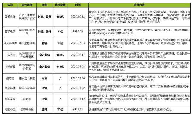
The government plays the role of venture capital and participates in the investment and construction of a large number of SiC projects.
Most SiC projects are jointly invested and constructed by local governments and enterprises. Local governments invest relatively more and bear more risks.
Unlike traditional Si-based projects that are concentrated in first- and second-tier cities in China, SiC projects are spread across the country.
Compared with Si-based projects, the overall investment in SiC projects is relatively low, and many small and medium-sized city governments are eager to improve the city's image and increase the layout of the semiconductor industry.
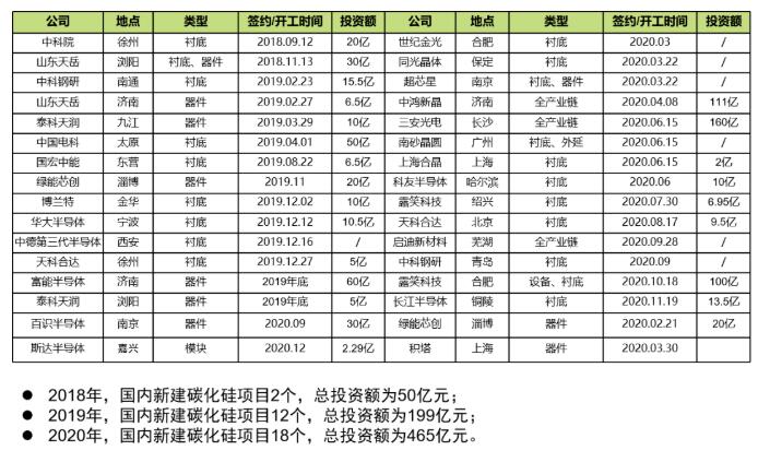
Summary of some SiC projects that local governments are specifically involved in
Capital enthusiasm is rising, and a large amount of money is pouring into the SiC industry.
The central and local governments have promulgated a series of policies to promote the development of the SiC industry.
In addition, in "Made in China 2025", the country has also put forward specific goals for the localization rate of 5G communications and efficient energy management. The target requires that the localization rate of advanced semiconductor materials should reach 50% by 2025. These favorable policies will greatly help the further development and growth of the SiC market.
At Lujing Semiconductor's participation in the 2021 Munich Electronics Show, the TV column group "Quality" also interviewed the company's general manager Mr. Xu Wenhui about "Made in China 2025" regarding the development of third-generation semiconductors. The application of silicon carbide power devices will be widely used in the next 3-5 years, and can even completely replace silicon-based products in some fields.
Compared with foreign markets, my country started research on SiC materials and devices relatively late. Driven by various factors, China's SiC industry chain has completed the basic layout and achieved certain results, gradually narrowing the gap with foreign advanced technologies. Several leading companies have emerged in every link.
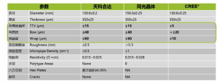
There is a clear gap between technical indicators and international manufacturers, and product consistency is a shortcoming that is difficult to overcome.
The reasons for the technology gap and consistency problems of domestic substrates can be roughly summarized into the following two categories:
Technical aspects such as material matching, equipment accuracy and thermal field control require a long period of know-how accumulation. Domestic manufacturers started relatively late and invested less, leaving a clear gap with leading foreign manufacturers. Domestic manufacturers have fewer and more scattered customers, and their feedback speed is slower and the feedback content is incomplete. CREE's product lines cover substrates, epitaxy, devices and even modules, and back-end feedback is sufficient and timely.
The technological gap directly leads to poor overall performance of the substrate and its inability to be used in production lines with higher requirements. The consistency problem means that the proportion of high-quality substrates is low, which directly leads to a significant increase in the cost of the substrates. Mainly because of the above two points, domestic substrates are currently unable to enter the mainstream supply chain.
Technical barriers are low, and the overall technical level is not much different from that of foreign countries.
The epitaxial technology is relatively simple, and the main process is to grow a new layer of single crystal on the original SiC substrate. It is a link with lower added value and lower technical threshold in the entire industrial chain.
The epitaxial process relies on mature equipment (currently the mainstream equipment in the industry is CVD equipment provided by Aixtron and other companies). The vapor deposition process is strictly controlled by flow meters. The industry and equipment vendors have relatively mature technologies.
Taking the domestic manufacturer Han Tiantian as an example, the technical level is not much different from that of Japan's Showa Denko, a leading international extension company. According to survey feedback, Hantian Tiancheng and Showa Denko have competed in multiple markets around the world.
There is a clear gap between technical indicators and international manufacturers. The consistency of products is a shortcoming that is difficult to overcome. It is still difficult for domestic substrates to enter the mainstream supply chain.
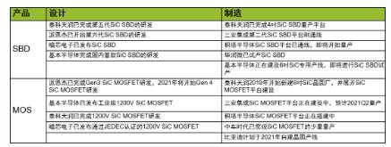
design:SiC device design is relatively simple, and the gap with foreign countries is relatively small
There are no patent barriers to SiC SBD device design. Leading domestic companies have begun the research and development of Gen 6 SiC SBD, and the gap with foreign countries is relatively small. In terms of SiC MOSFET devices, many domestic companies claim to have completed research and development, but have not yet entered mass production. At the same time, the latest Gen 4 Trench SiC MOSFET patent is held by foreign companies, and there may be patent issues in the future.
manufacture:There is a clear gap between SiC device manufacturing and foreign countries Most of the SiC SBD device manufacturing production lines are in a state of just opening up. They still need to go through stages such as production capacity ramping, and there is still a certain distance between large-scale and stable mass production. At present, all domestic SiC MOSFET device manufacturing platforms are still under construction, and the production lines of some companies are still in the planning stage, and there is still a long way to go before formal mass production.
Market competition is fierce, and the overall maturity of the domestic industry is still low.
The current competitive situation of domestic companies in SIC modules:
Many domestic new energy vehicle manufacturers have made radical layouts and built their own SiC module production lines to meet their own needs and cover them from upstream to downstream. At the same time, some traditional module manufacturers are also conducting research and development of SiC modules horizontally, relying on the experience of Si-based modules to speed up research and development progress.
However, most of the construction of module production lines of domestic new energy vehicle manufacturers started in 2019/20, and it will take at least 22 years to ramp up. Most of the emerging module manufacturers in China are small and have not yet achieved large-scale mass production. The maturity of domestic industry is still low.
In addition to competition among domestic manufacturers, the real competitive pressure in the SIC field still comes from foreign giants. Currently, 600-1700V silicon carbide SBDs and MOSFETs from major international manufacturers such as Infineon, ST, and Rohm have achieved mass production. Domestic silicon carbide manufacturers are currently mainly launching diode products. Only a handful of MOSFET manufacturers are mass-producing, and there is still room for breakthroughs. In terms of production lines, Cree, Infineon, etc. have begun to lay out 8-inch lines, while domestic manufacturers are still transitioning to 6-inch lines. Cree alone accounts for about 40% of the substrate market.
For a long time to come, the path of attack for domestic SIC industry chain companies will be on the horizon. There is still a long way to go! But fortunately, SiC has performed extremely well in various fields such as 5G, new energy vehicles, and photovoltaics. The market is large enough, and the demand for domestic substitution continues, so domestic companies can still compete!
Shandong Tianyue,Tianke Heda, Zhongke Energy Saving, Tongguang Crystal
Han Tian Tian Cheng,Dongguan Tianyu
Sanan Integration、Tyco Tianrun, Zhanxin Electronics, Basic Semiconductor、Jinan Lujing Semiconductorwait.
Disclaimer: This article is reproduced from "Lu Jingxin City". This article only represents the author's personal views and does not represent the views of Sacco Micro and the industry. It is only for reprinting and sharing and supports the protection of intellectual property rights. Please indicate the original source and author for reprinting. If there is any infringement, please contact us to delete it.
Related Recommendations
Exclusive Interview with Li Gang of Yunfan Ruida: The Precision of Millimeter-Wave Radar Products and the Warmth of Humanity
2026-07-22
2539
RF Passion, Craftsman’s Journey: Over 30 Years of Steadfast Dedication — Interview with Kinghelm Chief Engineer Mr. Qin hongxiang
2026-06-26
2701





 粤公网安备44030002007346号