
























Service Hotline
News

News
Not only lithography machines, these five semiconductor equipment giants control the "throat" of global chip manufacturing
2022-03-16
899
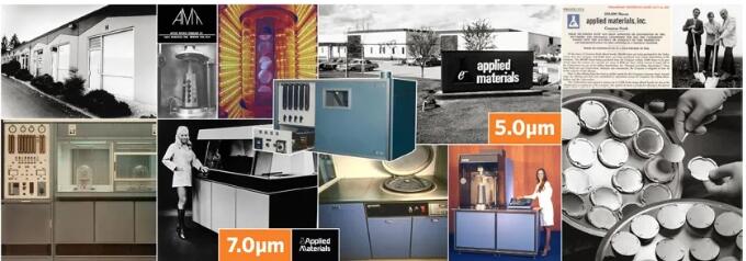
Applied Materials was founded in 1967 and is headquartered in Silicon Valley, USA. The founder is Michael McNeilly, who graduated from the Department of Chemistry at Gonzaga University and worked in the silicone department of union Carbide Electronics founded by Jean Hoerni, known as the "silicon transistor pioneer." Later, he set up his own company, Apogee Chemicals. In 1967, McNeilly left Apogee due to conflicts with his partners and borrowed $7,500 from his father-in-law as start-up capital to establish Applied Materials to produce semiconductor manufacturing equipment. It is worth mentioning that the U.S. semiconductor industry began to develop rapidly in 1967, and many executives and talents began to jump out of Fairchild Semiconductor to start their own businesses. Silicon Valley was dotted with various newly established semiconductor device manufacturers. Unlike traditional giants, these emerging semiconductor companies do not have internal production capabilities. Applied Materials took this opportunity to develop. In the first few years of its establishment, Applied Materials' revenue grew at an annual rate of more than 40%.
ASML mainly provides photolithography machines and related services to semiconductor manufacturers. Lithography machine, also known as mask alignment exposure machine, is the core equipment of the lithography process. The photolithography process is the most critical step in the chip manufacturing process. Photolithography can determine the key dimensions of the chip. This step also accounts for 35% of the overall chip manufacturing cost. As Intel, TSMC, Samsung and other companies enter the era of mass production focusing on advanced processes such as 7nm, every chip manufacturer hopes to purchase as many lithography machines as possible to increase production capacity. This has made ASML's limelight boom, with multiple performance indicators such as revenue hitting new highs.
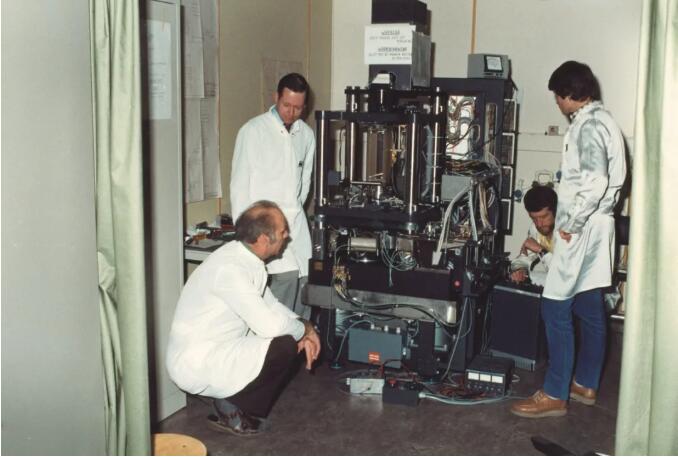
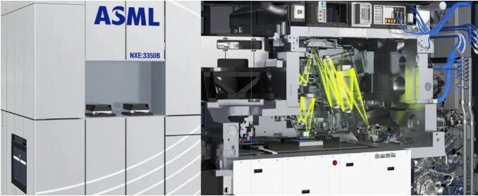
Since then, Asmai has made two leaps with the help of two "Bo Le". At the beginning of the 20th century, ASML andTSMCCooperated to develop a technical solution called "immersion lithography" and produced the first immersion lithography machine prototype in 2004, which enabled it to technically catch up with its competitor Nikon for the first time. In 2007, ASML captured 60% of the photolithography machine market, surpassing Nikon in revenue for the first time. As early as 1997,IntelIt has joined forces with governments and enterprises to establish EUV LLC, the top cutting-edge technology organization in the chip industry, to research and promote the development of EUV technology. EUV lithography uses shorter wavelengths of light to create smaller chips. ASML is a member of this organization and has obtained priority access to the United States' leading semiconductor technology. This step allows ASML to leave competitors such as Nikon far behind. In 2010, ASML delivered its first prototype extreme ultraviolet (EUV) lithography tool, and in 2015, ASML's EUV lithography process was ready for mass production. The output of ASML's EUV lithography machines has never been high, and the unit price is as high as 115 million euros. It is currently mainly provided to TSMC, Intel, Samsung Electronics and other companies. Japan’s No. 1 company that started its business through agency trade—Tokyo Electronics
Japanese companies still show a huge presence in the field of semiconductor manufacturing equipment, and Tokyo Electron Limited is one of the leaders. Tokyo Electronics was born in 1963. At that time, the company name was "Tokyo Electronics Laboratory Co., Ltd." and it was affiliated to Tokyo Broadcasting System Co., Ltd. Initially, Tokyo Electronics' registered capital was only 5 million yen, and there were only 6 employees including the founder. It was not until 1965 that it signed an agency contract with Fairchild Semiconductor in the United States for IC testers, and it began to develop. But Tokyo Electronics is by no means satisfied with being just an agent. In 1968, it established a joint venture company Tel Thermco with Thermco of the United States to produce and sell diffusion furnaces. This was also Japan's first semiconductor equipment manufacturer. In 1976, Tokyo Electronics developed the world's first high-pressure oxidation furnace; in 1986, the first vertical diffusion furnace was shipped. By 1989, Tokyo Electron's semiconductor manufacturing equipment revenue exceeded US$600 million, ranking first in the world and retaining the global championship for three consecutive years.

Tokyo Electronics' products cover almost all processes in the semiconductor manufacturing process. Tokyo Electronics holds 90% of the world's share in the field of "coating and developing equipment" that coats photoresist (photosensitive material) on wafers and displays electronic circuits. It also has advantages in fields such as "etching" that uses gas to remove excess parts other than circuits. In order to meet the growing demand for global semiconductors, Tokyo Electronics plans to promote investments such as research and development. Tokyo Electronics President Toshiki Kawai said that the company plans to invest 400 billion yen (approximately RMB 25 billion) in research and development funds in the three years starting from fiscal 2019 (ending March 2020). Tokyo Electron's goal is to become the world's largest supplier of semiconductor equipment. Leading the etching equipment market——Fanlin Group
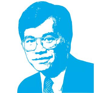
Lam Research, a leading semiconductor equipment company, was founded by David K. Lam, who was born in China. David K. Lam has worked at Xerox, Hewlett-Packard, and Texas Instruments. In 1980, he received financial support from Intel founder Bob Noyce and established Lam Group. Lam Group focuses on the etching, deposition and cleaning markets. In 1981, the first plasma etching machine product AutoEtch was launched; in 1992, the first ICP dry etching equipment was developed, opening the door to ICP etching equipment; in 2014, it entered the field of atomic layer etching; in 2020, it released innovative plasma etching technology and system solutions, which increased the etching output accuracy by more than 50%. Fanlin Group occupies half of the etching machine market.
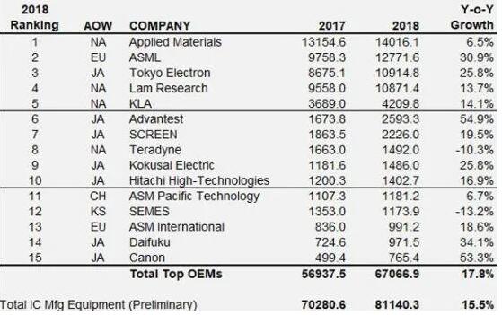
Lam Group’s business also spans the world. Since the mid-1980s, Lam Group has expanded globally, opening offices and establishing business in Europe, South Korea, Singapore, Japan, China, and India. From Lam's financial report, we can learn that the Asia-Pacific region contributes the most to its revenue, accounting for 80% of the total revenue. Last year, SMIC spent US$600 million to purchase capital equipment consisting of Lam etching tools for the production of wafer products. The king in the field of semiconductor testing equipment - Kelei SemiconductorKLA Semiconductor (KLA) was formed in 1997 by the merger of two companies, KLA and Tencor. The former was founded in 1975 and focuses on defect detection solutions; the latter was founded in 1977 and focuses on measurement solutions. After the merger, it was called KLA-Tencor Corporation and was renamed KLA Corporation in 2019. Although there is a big gap between Kelei and the top four manufacturers in terms of revenue level, according to SEMI statistics, Kelei accounted for more than half of Qiandao's detection and measurement market in 2018, ranking first in the industry.
Kelei Semiconductor has grown through a series of mergers and acquisitions. In 2019 alone, Kelei Semiconductor conducted 28 mergers and acquisitions, such as the acquisition of Israeli company Orbotech for approximately US$3.2 billion. Kelei Semiconductor has always been optimistic about the Chinese market. It established its first branch in China in 1999 and currently has 10 offices in Beijing, Shanghai, Nanjing, Xi'an, Wuhan, Tianjin, Shenzhen, Dalian, Xiamen, and Wuxi. In 2019, more than half of Kelei's revenue came from China.
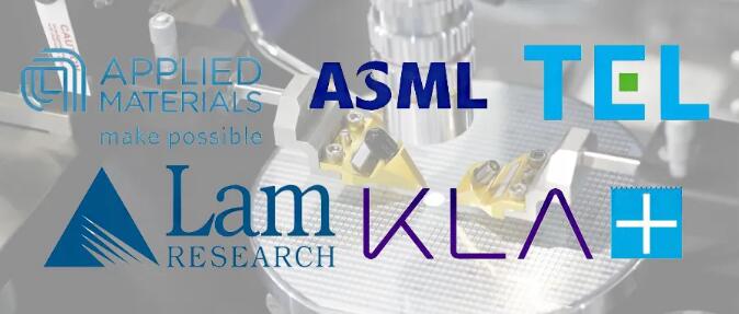
Although the world was hit by the COVID-19 epidemic in 2020 and many industries faced great challenges, semiconductor equipment manufacturers did not seem to suffer losses. The performance and stock prices of the five semiconductor equipment giants mentioned above almost all achieved considerable growth last year. Not long ago, at the opening ceremony of SEMICON China, Ju Long, global vice president and president of China of the International Semiconductor Industry Association (SEMI), revealed that the global semiconductor equipment market will grow significantly by 18.9% in 2020, and mainland China will grow by 39%, becoming the world's largest equipment market for the first time. The total revenue of these five equipment manufacturers in the mainland Chinese market in 2020 reached 72.7 billion yuan. Their CEOs have both said China is critical to their business and have pledged to work more closely with Chinese companies. When the technology industry encounters an unprecedented chip supply crisis, I believe that only global openness, cooperation and joint efforts are the right way forward for enterprises.
Disclaimer: This article is reproduced from "Global TMT", which supports the protection of intellectual property rights. Please indicate the original source and author when reprinting. If there is any infringement, please contact us to delete it.
Company phone number: +86-0755-83044319
Fax/FAX: +86-0755-83975897
Email: 1615456225@qq.com
QQ: 3518641314 Manager Li
QQ: 332496225 Manager Qiu
Address: Room 809, Building C, Zhantao Technology Building, No. 1079 Minzhi Avenue, Longhua New District, Shenzhen
Related Recommendations
Exclusive Interview with Li Gang of Yunfan Ruida: The Precision of Millimeter-Wave Radar Products and the Warmth of Humanity
2026-07-22
2510
RF Passion, Craftsman’s Journey: Over 30 Years of Steadfast Dedication — Interview with Kinghelm Chief Engineer Mr. Qin hongxiang
2026-06-26
2679





 粤公网安备44030002007346号