
























Service Hotline
News

News
Gallium oxide with unlimited potential
2022-03-16
1043
In that article, they expressed optimism about the prospects of gallium nitride in then-nascent broadband wireless networks, radar, and power switching applications for power grids. They also refer to GaN devices as"The most robust transistor ever created".
They are correct. GaN's wide bandgap (the energy required to break bound electrons and facilitate conduction) and other qualities allow us to exploit this material's high electric field tolerance, enabling devices with unprecedented performance.
Today, GaN is the undisputed champion of solid-state RF power applications, already showing up in radar, 5G wireless, and will soon become commonplace in power inverters used in electric vehicles. Now, you can even buy USB chargers designed based on GaN devices, which offer significantly high power levels in their compact size.
However, even if this is the case, we still ask, is there anything better than GaN? Is there anything that can be done to make an RF amplifier more powerful and efficient? Is there anything that can make power electronics shrink even further, further easing the burden on planes and cars? Can we find materials with larger band gaps that can still conduct electricity?
As it turns out, the answer is yes.
In fact, there are materials with many band gaps on the market, but the particularity of quantum mechanics means that most of them can hardly be used as semiconductors. However, there is one compelling candidate: the transparent conductive oxide gallium oxide (Ga2O3).
With its wide bandgap of nearly 5 eV, gallium oxide leads GaN (3.4eV) by a mile, and compared to silicon (1.1eV), the lead is as large as a marathon. We know that diamond and aluminum nitride also have large band gaps, but they do not have the properties that Ga2O3 does, which is a lucky set of properties that can be used to make cheap but powerful devices.
It is not enough for a material to have a wide bandgap, because if so, all dielectrics and ceramics can, which is why they can only be used as insulators. But gallium oxide has a unique combination of qualities that could make it very useful as a material candidate for power switches and RF electronics.
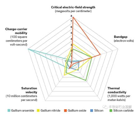
Illustration: IEEE Spectrum Source: “Implementation of Ga2O3 for Power Electronics Applications” presented by Gregg H. Jessen et al. at the 75th Annual Device Research Conference (DRC).
Among the five properties that are crucial to semiconductors, high critical electric field strength is the biggest advantage of beta-gallium oxide. This could help create high-voltage switches and could mean powerful RF devices can be designed based on them. However, the biggest disadvantage of beta-gallium oxide is its low thermal conductivity, which means heat can be trapped inside the device.
Also, a nice property of gallium oxide is that you can add charge carriers to it to make it more conductive through a process called doping. Doping involves adding controlled amounts of impurities to a crystal to control the concentration of charge carriers in the semiconductor. In silicon, for example, you can use ion implantation followed by annealing to dope the crystal with phosphorus (adding free electrons) or boron (subtracting them), allowing charges to move freely within it. In Ga2O3 you add electrons in a similar way.
But if you try to use this approach with other wide-bandgap oxides, you end up with potentially shattered crystals and spots in the lattice where charges get stuck.
Gallium oxide’s adaptability to the addition of dopants via standard processes (called ion implantation) as well as during epitaxial growth (depositing additional crystals) allows us to borrow from a number of established commercial lithography and processing technologies. These methods make it relatively easy to precisely define transistor dimensions in tens of nanometers and generate a variety of device topologies. However, other semiconductor materials with wide bandgaps do not have this incredibly useful feature. Not even GaN can do this.
Another advantage of gallium oxide is that, as these things go, large silicon wafers of crystalline Ga2O3 are actually very easy to fabricate. Although there are several types of Ga2O3 crystals, the most stable is called β, followed by ε and α. Among them, β-Ga2O3 has the most overall research, mainly due to the efforts of institutions such as the National Institute of Materials Science in Tsukuba, Japan and the Leibniz-Institut für Kristallzüchtung in Berlin.
The most attractive aspect of β-Ga2O3 is its thermal stability, which allows it to be manufactured using a number of already widely used techniques, including the Czochralski method for manufacturing silicon wafers. We can also use a crystal growth technique called edge-defined, film-fed. Nowadays, crystals can even be grown using the highly scalable vertical Bridgman-Stockbarger technique.
It’s difficult to overstate how different this situation is from other wide-bandgap semiconductors. However, from the current perspective, except for silicon carbide (SiC), most emerging wide-bandgap semiconductors do not have large-size substrates on which large crystals can be grown. This means they have to grow on a disk of another material, which comes at a cost. For example, gallium nitride is typically grown on silicon, silicon carbide or sapphire substrates in a complex process. But the crystal structure of these substrates is obviously different from that of GaN, and this difference can create a "lattice mismatch" between the substrate and GaN, resulting in a large number of defects. These defects caused many problems for the equipment produced. Because Ga2O3 acts as its own substrate, there are no mismatches and therefore no defects. Japan's Novel Crystal Technology has demonstrated 150 mm β-Ga2O3.
at the Japan Institute of Information and Communications Technology (NICT)Masataka Higashiwakiwas the first to realize the potential of β-Ga2O3 in power switching applications. In 2012, he shocked the entire power device field after his research group reported the first single-crystal β-Ga2O3 transistor. How good is this product? For example, one of the key specifications of a power transistor is breakdown voltage, a critical point at which the semiconductor's ability to stop the flow of current breaks down. The breakdown voltage of the pioneering transistor introduced by Higashiwaki is greater than 250V. For comparison, it took GaN nearly two decades to achieve this achievement.
In their seminal work, Higashiwaki described that they also significantly reduced the device's power losses by using a material with a high critical electric field strength. This characteristic, known as Ec, is gallium oxide's real superpower.
Simply put, if you sandwich a material between two conductors, and you increase the voltage, E c is the electric field at which the material starts to conduct electricity. Many times, this voltage can sometimes bring disastrous results. Silicon's critical field strength is typically measured in hundreds of kilovolts per centimeter, while Ga2O3's critical field strength is 8 megavolts per centimeter.
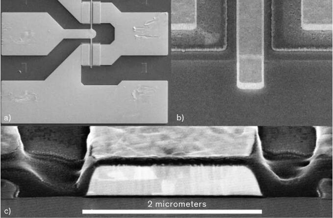
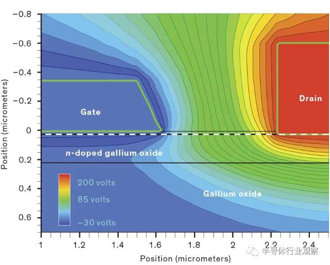
Image: Air Force Research Laboratory
High-voltage hero: This gallium oxide transistor pictured above (shown above at two magnifications (a and b) and in cross-section (c)) maintains voltages above 200 volts within just 600 nanometers.
When you think about ideal power switching transistors, having a very high E is one of the biggest attractions. Ideally, the device would switch instantaneously between two states: always on (conduction without resistance) and always off (no conduction at all). These two extremes have two very different device geometries. For the off state, you need to put a thicker layer of material between the source and drain of the transistor to prevent conduction and block large voltages. For the on state, you need an infinitely thin area so that it has no resistance.
Of course, you can't have both. The critical electric field strength of the material determines how thin the area can actually be made to still be closed.
The key indicator of low-frequency power switching semiconductors is called the Baliga figure of merit, named after IEEE Medal of Honor recipient B. Jayant Baliga. Essentially, it indicates how well the device's output reproduces the details of the input signal at high voltages. This is a very important property for transistors operating as switches at frequencies up to the kilohertz range. Such devices are found in multi-kilovolt substation equipment, high-energy photon generators for medical imaging, and power inverters for electric vehicles and industrial motor drives.
For all of these applications and more, Ga2O3 has natural advantages. At these frequencies, the quality factor is proportional to the cube of the critical electric field. Such a high E c means a good figure of merit.
Behind the math is the fact that this switch spends most of its time either fully on or fully off, and very little time switching between the two. So most of the power loss is just the current from the resistor to when the device is turned on. When E c is high, thinner devices can be used, which means less resistance.
The message of Higashiwaki's work is simple: You can use powerful high electric field strengths to achieve high-voltage switching that loses little power at low frequencies. Other research groups soon got the message. By 2013, researchers had demonstrated a metal-oxide-semiconductor field-effect transistor (MOSFET) with a breakdown voltage of 370V. In 2016, Man Hoi Wong, then part of NICT's Higashiwaki group, used an additional structure called field plating to push the voltage above 750V. Among these devices, the relative ease with which Ga2O3 can achieve higher operating voltages is indeed remarkable. Research into materials has come a long way in just a few years, whereas GaN leaf took decades.
Would Ga2O3 be useful in fast switching power supply applications? This is another point that everyone pays attention to. It needs to be emphasized that E c is also very important here and may bring great advantages to Ga2O3.
At higher frequencies (such as 100 Hz to 1 MHz), the time it takes a device to turn on and off increases proportionally. The losses during switching are the product of the device resistance and how much charge needs to accumulate on the transistor gate to switch. Doing the math, this means that the losses are proportional to the square of the critical electric field strength, not the cube at low frequencies.
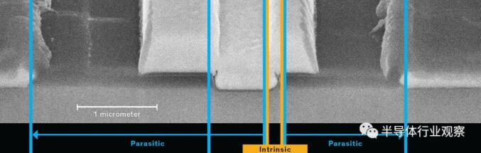 Image: Air Force Research Laboratory
 The picture above shows the gallium oxideRF application potential,A small part (intrinsic) of this early gallium oxide RF transistor was important to its operation. Reducing the parasitic resistance in the device can increase power and frequency.
You will find that in an application as simple as a mobile phone charger, faster power switching will bring more benefits. A switching power supply works by first rectifying the AC voltage from the wall plug and then chopping it into a high-frequency signal. The transformer reduces the voltage to the required level and finally the signal is rectified and filtered. The most bulky parts of the system are the transformers and other passive components, and smaller components can only be used as the frequency is increased. And if you want higher frequencies, a semiconductor with a wider band gap and a higher critical electric field will allow you to get it more efficiently while also simplifying heat dissipation.
For example, a 1200V silicon inverter switching at 20kHz can provide approximately 3kW of power. However, by switching at 150kHz, a silicon carbide inverter delivering the same power can operate at a higher temperature in a package that is one-third the size. As a comparison, Ga2O3-based inverters can operate at frequencies close to megahertz and can be half as small (although this would require magnetic components that have not yet been invented).
So, in summary, the true electronic properties of materials such as Ga2O3 come from fully utilizing their critical electric field strength. But what exactly is that value? Until 2015, no group had conducted actual measurements of the field strengths achievable by the material. As with other devices, preliminary results are far from theoretical limits.
My colleagues and I are facing this challenge while working at the Air Force Research Laboratory at Wright-Patterson Air Force Base, Ohio. The first problem we encountered was that any device made using materials with such high field strengths had the potential to exceed the limits of existing test equipment. Because in principle, 2 micron materials may block more than 1.5kV! So we built a simple MOSFET whose geometry was scaled down to reduce the voltage. The gap between gate and drain where the electric field is highest is only 600 nanometers. This is partly to make measuring peak E c easier, but also because we want to be able to test the device at RF frequencies, which larger high voltage designs don't allow for.
In this early demonstration, the transistors were able to withstand 230V, which is the limit of RF test equipment. The average electric field generated is at least 3.8 MV/cm, and simulations show that the peak internal electric field is at least 5.3 MV/cm. (We will never observe the full 8MV/cm in a FET) This is the first experimental demonstration that Ga2O3 has a larger theoretical E C value than GaN (around 3.3MV/cm). To put it another way, the gate-to-drain gap of a GaN power transistor with a rated operating voltage of 600V is usually about 15 to 20 µm, and our wavelength is 600nm.
After this conclusion was made, power switching transistors developed at an alarming rate. In 2017, we manufactured MOSFETs with breakdown voltages greater than 600V. In early 2018, high-frequency loss values achieved using MOSFETs of different geometries met or exceeded the theoretical limits of silicon. What's more, we now have a clear path toward matching or exceeding the latest GaN values in the next few years.
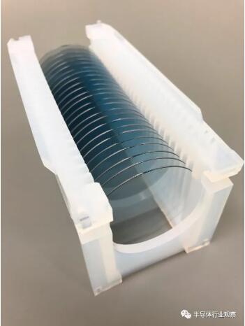 Photo: Novel Crystal Technology
 Unlike many wide-bandgap semiconductors, gallium oxide wafers can be made using roughly the same process as silicon wafers. Therefore, this means that defect-free devices may become relatively cheap.
When we measured the E of power switches in 2015, we also speculated that Ga2O3 might find similar success in RF circuits, again by allowing higher electric fields in smaller devices. But at that time, some key information was missing—there were no published data on the electron velocity in the material as a function of the electric field.
Electron speed is particularly important in transistors used to amplify radio frequency signals. In RF, high power output and high frequency are the goals, and Johnson’s figure of merit (JFOM) summarizes these goals. JFOM says that the product of power and frequency of an RF transistor is proportional to the product of the maximum velocity of charge carriers in the semiconductor material and Ec. The key thing we need to know here is that in an RF transistor you only get amplification if the carriers are able to make it flow all the way from source to drain before the polarity of the RF waveform switches. (The highest frequency at which this occurs is called the unit current gain frequency, or f T.)
Again, the high critical electric field of Ga2O3 comes into play because you can reduce that critical distance but still provide a strong electric field to accelerate electrons to their maximum speed.
At AFRL we managed to demonstrate the first submicron gallium oxide RF MOSFET in 2017. These devices put up some impressive numbers, although they're not at the top of the GaN league. Their unit current gain frequency is 3GHz, their maximum oscillation frequency is 13GHz, and their output power density is 230 mW/mm at 800MHz. Since then, AFRL’s pulsed RF power output density has exceeded 500mW/mm at 1GHz, with a maximum oscillation frequency approaching 20GHz.
Even more encouraging, around the same time, theoretical calculations by Krishnandu Ghosh and Uttam Singisetti (University of Buffalo) showed that JFOMs of gallium oxide are significantly better than those of gallium nitride.
Since the first demonstration of RF capabilities in 2017, RF Ga2O3 technology has made tremendous progress, first with Sriram Krishnamoorthy and then with Siddharth Rajan’s team at The Ohio State University demonstrating new and improved doping techniques. These technologies are borrowed from silicon, so the resulting resistance in the sheet of material where conduction occurs is very low, around 300 ohms per square. (Yes, that's the correct unit.) This is comparable to what you'll find in gallium nitride devices. Shortly after achieving this result, Rajan and researchers at the University of California, Santa Barbara, independently demonstrated Ga2O3 as a high electron mobility transistor (HEMT). D: agHEMT
This type of device is usually made from gallium arsenide or gallium nitride, and radio frequencies are critical for both cell phones and satellite TV receivers. Such devices conduct through a two-dimensional electron gas that forms at the sharp interface between two semiconductors with different band gaps. In this case, it's aluminum gallium oxide and gallium oxide, which is exactly similar to the commercial aluminum gallium arsenide/gallium arsenide HEMT technology in smartphones. These key breakthroughs provide a path for vertical and horizontal expansion of RF equipment.
Although these advances are encouraging, Ga2O3 is unlikely to challenge gallium arsenide (GaAs) or GaN in every RF application. As a fundamentally good switch, we expect it to have advantages in switch-mode amplifiers such as Class D, E, or F. Among these devices, the device has very low on-resistance and can achieve very high efficiency using low current, high breakdown voltage characteristics. On the other hand, device applications requiring lower impedance and high current will favor GaN, mainly due to its higher charge carrier mobility and charge carrier density.
SoGa2O3What challenges will it face?
Now, consider this: To get a true comparison of a material's thermal conductivity to a device, you need to normalize it to the material's ability to handle power. In other words, you need to divide E by C to accurately compare thermal issues in real devices. When you do that, you find that every semiconductor with a bandgap larger than silicon has heat dissipation issues when reaching its full potential, even diamond. While this fact still doesn't help Ga2O3 much, it motivates us to try to find better ways to dissipate heat.
For example, researchers at Tokyo's NICT Laboratory greatly improved the device's thermal resistance by bonding p-type polycrystalline SiC to the backside of a Ga2O3 silicon wafer as thin as about 10 microns. And, noting that for certain device topologies, virtually all the heat is generated in the top 1µm of the material, AFRL researchers obtained encouraging results simulating the effect of electrode contact and using dielectric fillers to shunt the heat to a heat sink. This is the trick used today in commercial gallium arsenide heterojunction bipolar transistors. So despite the thermal challenges in Ga2O3, smart engineers are working on it.
Another, more fundamental problem is that we can only make gallium oxide conduct electrons rather than holes. No one can make a good p-type conductor out of Ga2O3. And, frustratingly, the material's basic electronic properties don't hold much promise. In particular, the hole conduction shape in the valence band portion of the material's band structure is incorrect. Therefore, even if there is some kind of dopant that causes the receptor to be at the correct energy level, any holes created are expected to trap themselves before they can contribute to conduction. When theory and data are so consistent, it's hard to say there's a way around this shortcoming.
While this vulnerability does create additional challenges, it's not all plain sailing. Many so-called majority-carrier-only devices have been commercially successful. As an example, just look at as many USB-C wall chargers as you can get.
The research phase of Ga2O3 device technology has just begun to reach critical mass, and we are now planning the application space for fast switching, multi-kilovolt power transistors and RF devices. New demonstrations of kilovolt-class equipment are now also appearing regularly. RF transistors with critical dimensions in the tens of nanometers are about to become available. As we advance this technology, we think we will be able to achieve device topologies that have not been possible before in any other material.
Of course, we're going to break a few things (mainly dielectrics) as we go along. But that’s the definition of disruptive technology. We trade what we know for potential performance. Currently, for Ga2O3, the performance potential greatly outweighs the problems.
Disclaimer: This article is reproduced from "Semiconductor Industry Observation", which supports the protection of intellectual property rights. Please indicate the original source and author of the reprint. If there is any infringement, please contact us to delete it.
Company phone number: +86-0755-83044319
Fax/FAX: +86-0755-83975897
Email: 1615456225@qq.com
QQ: 3518641314 Manager Li
QQ: 332496225 Manager Qiu
Address: Room 809, Building C, Zhantao Technology Building, No. 1079 Minzhi Avenue, Longhua New District, Shenzhen
Related Recommendations
Exclusive Interview with Li Gang of Yunfan Ruida: The Precision of Millimeter-Wave Radar Products and the Warmth of Humanity
2026-07-22
2511
RF Passion, Craftsman’s Journey: Over 30 Years of Steadfast Dedication — Interview with Kinghelm Chief Engineer Mr. Qin hongxiang
2026-06-26
2679





 粤公网安备44030002007346号