
























Service Hotline
News

News
Summary of 70 semiconductor packaging forms!
2022-03-16
1394
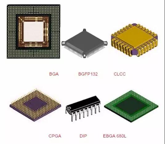
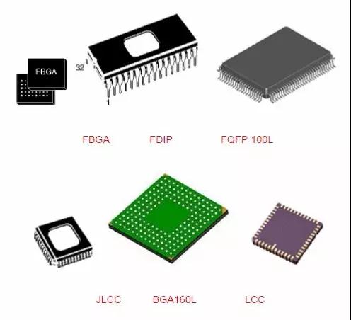
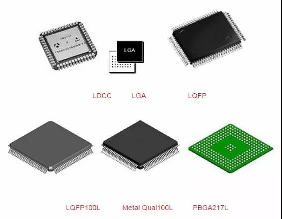
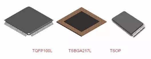
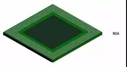
1、BGA(ball grid array)
Spherical contact arrangement, one of the surface mount packages. Spherical bumps are made in an array on the back of the printed circuit board to replace pins, an LSI chip is assembled on the front of the printed circuit board, and then sealed with molding resin or potting. Also known as bump placement carrier (PAC). The number of pins can exceed 200, and it is a package used for multi-pin LSI. The package body can also be made smaller than QFP (four-side pin flat package). For example, a 360-pin BGA with a pin center distance of 1.5mm is only 31mm square; while a 304-pin QFP with a pin center distance of 0.5mm is 40mm square. And BGA doesn't have to worry about pin deformation problems like QFP. This package was developed by the American Motorola Company and was first used in portable phones and other equipment. It may be popularized in personal computers in the United States in the future. Initially, the BGA's pin (bump) center distance was 1.5mm and the number of pins was 225. Now some LSI manufacturers are developing 500-pin BGA. The problem with BGA is the visual inspection after reflow. It is unclear whether the visual inspection method is effective. Some believe that due to the large center distance of welding, the connection can be regarded as stable and can only be handled through functional inspection. The American Motorola Company calls the package sealed with molded resin OMPAC, and the package sealed by potting method is called GPAC (see OMPAC and GPAC).
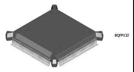
2、BQFP(quad flat package with bumper)
Cushioned four-side lead flat package. One of the QFP packages, protrusions (cushion pads) are provided at the four corners of the package body to prevent the leads from bending and deforming during transportation. American semiconductor manufacturers mainly use this package in circuits such as microprocessors and ASICs. The pin center distance is 0.635mm, and the number of pins ranges from about 84 to 196 (see QFP).
3. Butt joint pin grid array (PGA)
Another name for surface mount PGA (see surface mount PGA).
4、C-(ceramic)
Symbol indicating ceramic package. For example, CDIP stands for Ceramic DIP. It is a notation that is often used in practice.
5、Cerdip
Glass-sealed ceramic dual-in-line package for ECL RAM, DSP (Digital Signal Processor) and other circuits. Cerdip with glass window is used for UV erasable EPROM and microcomputer circuits with EPROM inside. The pin center distance is 2.54mm, and the number of pins is from 8 to 42. In Japan, this package is represented as DIP-G (G means glass seal).
6、Cerquad
One of the surface mount packages, a ceramic QFP with lower seal, used to package logic LSI circuits such as DSP. Cerquad with windows is used to encapsulate EPROM circuits. The heat dissipation is better than that of plastic QFP, and it can tolerate 1. 5 ~ 2W power under natural air cooling conditions. However, the packaging cost is 3 to 5 times higher than that of plastic QFP. The pin center distance has various specifications such as 1.27mm, 0.8mm, 0.65mm, 0.5mm, 0.4mm and so on. The number of pins ranges from 32 to 368.
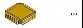
7、CLCC(ceramic leaded chip carrier)
Ceramic chip carrier with pins, one of the surface mount packages, the pins are led out from the four sides of the package in a T-shape. Those with windows are used to package UV-erasable EPROMs and microcomputer circuits with EPROMs. This package is also called QFJ, QFJ-G (see QFJ).
8、COB(chip on board)
Chip packaging on board is one of the bare chip mounting technologies. Semiconductor chips are hand-mounted on a printed circuit board. The electrical connection between the chip and the substrate is achieved by wire stitching. The electrical connection between the chip and the substrate is achieved by wire stitching and covered with resin to ensure reliability. Although COB is the simplest bare chip mounting technology, its packaging density is far inferior to TAB and flip-chip soldering technologies.
9、DFP(dual flat package)
Double sided flat package. Is another name for SOP (see SOP). This term used to be used in the past, but it is basically no longer used.
10、DIC(dual in-line ceramic package)
Another name for ceramic DIP (including glass seal) (see DIP).
11、DIL(dual in-line)
Another name for DIP (see DIP). European semiconductor manufacturers often use this name.
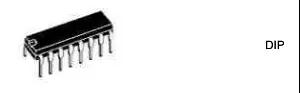
12、DIP(dual in-line package)
Dual in-line package. One of the plug-in packages, the pins are led out from both sides of the package. The packaging materials are plastic and ceramic. DIP is the most popular plug-in package, and its application range includes standard logic IC, memory LSI, microcomputer circuits, etc. The pin center distance is 2.54mm, and the number of pins ranges from 6 to 64. Package width is typically 15.2mm. Some packages with widths of 7.52mm and 10.16mm are called skinny DIP and slim DIP (narrow DIP) respectively. But in most cases, no distinction is made and they are simply collectively referred to as DIP. In addition, ceramic DIP sealed with low melting point glass is also called cerdip (see cerdip).
13、DSO(dual small out-lint)
Double sided pin small outline package. Another name for SOP (see SOP). Some semiconductor manufacturers use this name.
14、DICP(dual tape carrier package)
Double sided lead loaded package. One of TCP (load encapsulation). The pins are made on insulating tape and lead out from both sides of the package. Because it uses TAB (automatic load soldering) technology, the package appearance is very thin. It is often used in liquid crystal display driver LSI, but most of them are customized products. In addition, a 0.5mm thick memory LSI book-shaped package is in the development stage. In Japan, DICP is named DTP in accordance with the standards of the EIAJ (Electronic Machinery Industry of Japan) Association.
15、DIP(dual tape carrier package)
Same as above. The naming of DTCP is based on the Japan Electronics Machinery Industry Association standard (see DTCP).
16、FP(flat package)
Flat pack. One of the surface mount packages. Another name for QFP or SOP (see QFP and SOP). Some semiconductor manufacturers use this name.
17、flip-chip
Flip solder the chip. One of the bare chip packaging technologies, metal bumps are made in the electrode area of the LSI chip, and then the metal bumps are pressure-welded and connected to the electrode area on the printed substrate. The footprint of the package is basically the same as the chip size. It is the smallest and thinnest among all packaging technologies. However, if the thermal expansion coefficient of the substrate is different from that of the LSI chip, a reaction will occur at the joint, affecting the reliability of the connection. Therefore, it is necessary to reinforce the LSI chip with resin and use substrate materials with basically the same thermal expansion coefficient.
18、FQFP(fine pitch quad flat package)
Small pin center distance QFP. Usually refers to QFP with a pin center distance less than 0.65mm (see QFP). Some conductor manufacturers use this name.
19、CPAC(globe top pad array carrier)
The American Motorola Company's nickname for BGA (see BGA).
20、CQFP(quad fiat package with guard ring)
Four-sided pin flat package with guard ring. One of the plastic QFPs, the pins are shielded with resin protective rings to prevent bending and deformation. Before assembling the LSI on the printed circuit board, cut the pins from the guard ring and make them into a gull wing shape (L shape). This kind of package has been mass-produced by Motorola Company in the United States. The pin center distance is 0.5mm, and the maximum number of pins is about 208.
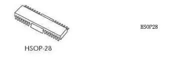
21、H-(with heat sink)
Indicates mark with radiator. For example, HSOP means SOP with heat sink.
22、pin grid array(surface mount type)
Surface mount PGA. Usually PGA is a plug-in package with a pin length of about 3.4mm. Surface mount PGAs have array-like pins on the bottom of the package, with lengths ranging from 1.5mm to 2.0mm. Mounting adopts the method of butt welding with the printed circuit board, so it is also called butt welding PGA. Because the pin center distance is only 1.27mm, which is half smaller than the plug-in type PGA, the package body can be made not very large, and the number of pins is more than that of the plug-in type (250~528). It is a package for large-scale logic LSI. The substrates for packaging include multi-layer ceramic substrates and glass epoxy resin printed bases. The use of multi-layer ceramic substrates to make packages has become practical.
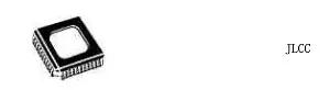
23、JLCC(J-leaded chip carrier)
J-pin chip carrier. Another name for windowed CLCC and windowed ceramic QFJ (see CLCC and QFJ). A name adopted by some semiconductor manufacturers.
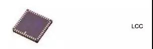
24、LCC(Leadless chip carrier)
Leadless chip carrier. Refers to a surface mount package in which only electrodes are in contact on the four sides of the ceramic substrate and there are no leads. It is a package for high-speed and high-frequency ICs, also called ceramic QFN or QFN-C (see QFN).
25、LGA(land grid array)
Contact display package. That is, a package with flat electrode contacts in an array state is made on the bottom surface. Just plug it into the socket during assembly. Ceramic LGAs with 227 contacts (1.27mm center distance) and 447 contacts (2.54mm center distance) are now available for use in high-speed logic LSI circuits. Compared with QFP, LGA can accommodate more input and output pins in a smaller package. In addition, since the impedance of the lead is small, it is very suitable for high-speed LSI. However, due to the complexity and high cost of making sockets, they are basically not used nowadays. The demand for it is expected to increase in the future.
26、LOC(lead on chip)
On-chip leaded packaging. One of the LSI packaging technologies, a structure in which the front end of the lead frame is above the chip. A bump solder joint is made near the center of the chip, and the electrical connection is made with lead stitching. Compared with the original structure of arranging the lead frame near the side of the chip, the width of the chip accommodated in the same size package is about 1mm.
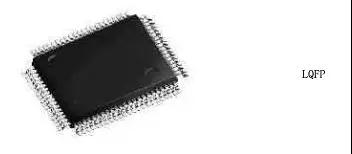
27、LQFP(low profile quad flat package)
Thin QFP. Refers to QFP with a package body thickness of 1.4mm. It is the name used by the Japan Electronics Machinery Industry Association based on the new QFP form factor.
28、L-QUAD
One of the ceramic QFP. The packaging substrate is made of aluminum nitride, which has a thermal conductivity 7 to 8 times higher than that of alumina and has better heat dissipation. The frame of the package is made of aluminum oxide and the chip is sealed using a potting method, thus keeping costs down. It is a package developed for logic LSI and can tolerate W3 power under natural air cooling conditions. 208-pin (0.5mm center distance) and 160-pin (0.65mm center distance) LSI logic packages have been developed and mass production began in October 1993.
29、MCM(multi-chip module)
Multi-chip components. A package in which multiple bare semiconductor chips are assembled on a wiring substrate. According to the substrate material, it can be divided into three categories: MCM-L, MCM-C and MCM-D. MCM-L is a module using a common glass epoxy resin multilayer printed circuit board. The wiring density is not very high and the cost is low. MCM-C is a component that uses thick film technology to form multi-layer wiring and uses ceramic (alumina or glass ceramic) as the substrate. It is similar to thick film hybrid ICs that use multi-layer ceramic substrates. There is no obvious difference between the two. The wiring density is higher than MCM-L. MCM-D is a component that uses thin film technology to form multi-layer wiring and uses ceramic (aluminum oxide or aluminum nitride) or Si or Al as the substrate. The wiring conspiracy is the highest among the three components, but the cost is also high.
30、MFP(mini flat package)
Small flat package. Another name for plastic SOP or SSOP (see SOP and SSOP). A name adopted by some semiconductor manufacturers.
31、MQFP(metric quad flat package)
A classification of QFP according to JEDEC (Joint Electronics Equipment Council) standards. Refers to the standard QFP with a pin center distance of 0.65mm and a body thickness of 3.8mm to 2.0mm (see QFP).
32、MQUAD(metal quad)
A QFP package developed by the American Olin Company. The base plate and cover are made of aluminum and sealed with adhesive. Under natural air cooling conditions, the power of 2.5W ~ 2.8W can be tolerated. Japan's Shinko Electric Industrial Co., Ltd. obtained a license to start production in 1993.
33、MSP(mini square package)
Another name for QFI (see QFI), often called MSP in the early stages of development. QFI is the name specified by the Japan Electronics Machinery Industries Association.
34、OPMAC(over molded pad array carrier)
Molded resin sealed bump display carrier. The name adopted by American Motorola Company for molded resin sealed BGA (see BGA).
35、P-(plastic)
A symbol indicating plastic packaging. For example, PDIP means plastic DIP.
36、PAC(pad array carrier)
Bump display carrier, another name for BGA (see BGA).
37、PCLP(printed circuit board leadless package)
Printed circuit board leadless packaging. The name adopted by Japan's Fujitsu Company for plastic QFN (plastic LCC) (see QFN). There are two specifications for pin center distance: 0.55mm and 0.4mm. Currently in the development stage.
38、PFPF(plastic flat package)
Plastic flat pack. Another name for plastic QFP (see QFP). A name adopted by some LSI manufacturers.
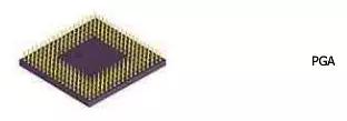
39、PGA(pin grid array)
Display pin package. One of the plug-in packages, the vertical pins on the bottom surface are arranged in an array. The packaging substrate basically uses multi-layer ceramic substrates. If the material name is not specifically indicated, most of them are ceramic PGAs, which are used in high-speed large-scale logic LSI circuits. The cost is higher. The pin center distance is usually 2.54mm, and the number of pins ranges from about 64 to 447. In order to reduce costs, the packaging substrate can be replaced by a glass epoxy resin printed substrate. There are also plastic PGAs with 64 to 256 pins. In addition, there is a short-lead surface-mount PGA (butt-soldering PGA) with a pin center distance of 1.27mm. (See Surface Mount PGA).
40、piggy back
Piggyback packaging. Refers to a ceramic package equipped with a socket, similar in shape to DIP, QFP, and QFN. Used to evaluate program verification operations when developing equipment with microcomputers. For example, plug the EPROM into the socket for debugging. This kind of packaging is basically a customized product and is not very popular in the market.
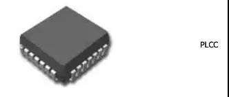
41、PLCC(plastic leaded chip carrier)
Plastic chip carrier with leads. One of the surface mount packages. The pins are led out from the four sides of the package, in a T-shape, and are made of plastic. Texas Instruments Company of the United States first adopted it in 64k-bit DRAM and 256kDRAM, and now it has been widely used in logic LSI, DLD (or program logic device) and other circuits. The pin center distance is 1.27mm, and the number of pins ranges from 18 to 84. J-shaped pins are not easily deformed and are easier to operate than QFP, but visual inspection after welding is more difficult. PLCC is similar to LCC (also known as QFN). Previously, the only difference between the two was that the former used plastic and the latter used ceramic. But now there are J-shaped lead packages made of ceramics and leadless packages made of plastic (marked as plastic LCC, PC LP, P-LCC, etc.), and it is no longer possible to distinguish them. For this reason, the Japan Electronics Machinery Industry Association decided in 1988 to call a package with J-shaped pins from four sides QFJ, and a package with electrode bumps on four sides called QFN (see QFJ and QFN).
42、P-LCC(plastic teadless chip carrier)(plastic leaded chip currier)
Sometimes it is another name for plastic QFJ, sometimes it is another name for QFN (plastic LCC) (see QFJ and QFN). Some LSI manufacturers use PLCC to indicate leaded packaging and P-LCC to indicate leadless packaging to show the difference.
43、QFH(quad flat high package)
Four-side lead thick body flat package. A type of plastic QFP. In order to prevent the package body from breaking, the QFP body is made thicker (see QFP). A name adopted by some semiconductor manufacturers.
44、QFI(quad flat I-leaded packgac)
Four-sided I-pin flat package. One of the surface mount packages. The pins are led out from the four sides of the package in an I shape downward. Also called MSP (see MSP). The mounting and printed circuit board are connected by butt welding. Since the pins have no protruding parts, the mounting area is smaller than that of QFP. Hitachi Manufacturing Co., Ltd. developed and used this package for video analog ICs. In addition, Japan's Motorola Company's PLL IC also uses this kind of packaging. The pin center distance is 1.27mm, and the number of pins ranges from 18 to 68.
45、QFJ(quad flat J-leaded package)
Four-sided J-shaped flat package. One of the surface mount packages. The pins are led out from the four sides of the package in a J-shaped downward direction. It is a name specified by the Japan Electronics Machinery Industries Association. The pin center distance is 1.27mm.
The materials are plastic and ceramic. Plastic QFJ is called PLCC in most cases (see PLCC) and is used in microcomputers, gate displays, DRAM, ASSP, OTP and other circuits. Pin count ranges from 18 to 84.
Ceramic QFJ is also called CLCC, JLCC (see CLCC). Windowed packages are used for UV-erasable EPROMs and microcomputer chip circuits with EPROMs. The number of pins ranges from 32 to 84.
46、QFN(quad flat non-leaded package)
Flat package with no leads on four sides. One of the surface mount packages. Now it is often called LCC. QFN is the name specified by the Japan Electronics Machinery Industry Association. There are electrode contacts on the four sides of the package. Since there are no leads, the mounting area is smaller than QFP and the height is lower than QFP. However, when stress occurs between the printed circuit board and the package, it cannot be relieved at the electrode contact. Therefore, it is difficult to make as many electrode contacts as there are QFP pins, usually from 14 to 100. There are two types of materials: ceramic and plastic. When there is an LCC mark, it is basically ceramic QFN. The center distance between electrode contacts is 1.27mm.
Plastic QFN is a low-cost package based on glass epoxy resin printed substrate. In addition to 1.27mm, the electrode contact center distance also has two types: 0.65mm and 0.5mm. This kind of packaging is also called plastic LCC, PCLC, P-LCC, etc.
47、QFP(quad flat package)
Four-side pin flat package. One of the surface mount packages, the pins are led out from four sides in a gull wing (L) shape. There are three types of base materials: ceramic, metal and plastic. In terms of quantity, plastic packaging accounts for the vast majority. When no material is specified, plastic QFP is used in most cases. Plastic QFP is the most popular multi-pin LSI package. Not only used in digital logic LSI circuits such as microprocessors and gate arrays, but also in analog LSI circuits such as VTR signal processing and audio signal processing. The pin center distance has various specifications such as 1.0mm, 0.8mm, 0.65mm, 0.5mm, 0.4mm, 0.3mm, etc. The maximum number of pins in the 0.65mm center distance specification is 304.
In Japan, QFP with pin center distance less than 0.65mm is called QFP (FP). But now the Japan Electronics Machinery Industry Association has re-evaluated the form factor of QFP. There is no distinction in the pin center distance, but according to the thickness of the package body, it is divided into three types: QFP (2.0mm ~ 3.6mm thick), LQFP (1.4mm thick) and TQFP (1.0mm thick).
In addition, some LSI manufacturers refer to QFP with a pin center distance of 0.5mm as shrink-type QFP or SQFP or VQFP. However, some manufacturers call QFP with pin center distances of 0.65mm and 0.4mm also called SQFP, which makes the name a little confusing. The disadvantage of QFP is that when the pin center distance is less than
At 0.65mm, the pins are prone to bending. To prevent pin deformation, several improved QFP varieties have emerged. For example, BQFP with tree finger cushions at the four corners of the package (see BQFP); GQFP with a resin protection ring covering the front of the pin (see GQFP); TPQFP that can be tested by setting test bumps in the package body and placing them in a special fixture to prevent lead deformation (see TPQFP). In terms of logic LSI, many development products and high-reliability products are packaged in multi-layer ceramic QFP. Products with a minimum pin center distance of 0.4mm and a maximum pin count of 348 are also available. In addition, glass-sealed ceramic QFPs are also available (see Gerqa d).
48、QFP(FP)(QFP fine pitch)
Small center distance QFP. The name specified by the standards of the Japan Electronics Machinery Industries Association. Refers to QFP with pin center distances of 0.55mm, 0.4mm, 0.3mm, etc. less than 0.65mm (see QFP).
49、QIC(quad in-line ceramic package)
Another name for ceramic QFP. The name used by some semiconductor manufacturers (see QFP, Cerquad).
50、QIP(quad in-line plastic package)
Another name for plastic QFP. The name used by some semiconductor manufacturers (see QFP).
51、QTCP(quad tape carrier package)
Four-side lead-loaded package. One of the TCP packages, the pins are formed on the insulating tape and lead out from the four sides of the package. It is a thin package using TAB technology (see TAB, TCP).
52、QTP(quad tape carrier package)
Four-side lead-loaded package. The name used for the form factor specifications established by the Japan Electronics Machinery Industry Association in April 1993 for QTCP (see TCP).
53、QUIL(quad in-line)
Another name for QUIP (see QUIP).
54、QUIP(quad in-line package)
Four rows of pins in a plug-in package. The pins are led out from both sides of the package, and every other pin is staggered and bent downward into four columns. The pin center distance is 1.27mm. When inserted into the printed circuit board, the insertion center distance becomes 2.5mm. Therefore it can be used on standard printed circuit boards. It is a smaller package than standard DIP. NEC uses several types of packages in microcomputer chips for desktop computers and home appliances. There are two types of materials: ceramic and plastic. The number of pins is 64.
55、SDIP (shrink dual in-line package)
Shrinkable DIP. One of the plug-in packages, the shape is the same as DIP, but the pin center distance (1.778mm) is smaller than DIP (2.54 mm).
Hence the name. Pin count ranges from 14 to 90. It is also called SH-DIP. There are two types of materials: ceramic and plastic.
56、SH-DIP(shrink dual in-line package)
Same as SDIP. A name adopted by some semiconductor manufacturers.
57、SIL(single in-line)
Another name for SIP (see SIP). European semiconductor manufacturers mostly use the name SIL.
58、SIMM(single in-line memory module)
Single rank memory component. A memory component equipped with electrodes only near one side of a printed circuit board. Usually refers to the component that plugs into the socket. Standard SIMM has two specifications: 30 electrodes with a center distance of 2.54mm and 72 electrodes with a center distance of 1.27mm. SIMMs with SOJ-packaged 1-megabit and 4-megabit DRAM installed on one or both sides of a printed circuit board have been widely used in personal computers, workstations and other equipment. At least 30 to 40% of DRAM is installed in SIMM.
59、SIP(single in-line package)
Single in-line package. The pins come out from one side of the package and are arranged in a straight line. When assembled onto a printed circuit board, the package stands on its side. The pin center distance is usually 2.54mm, and the number of pins ranges from 2 to 23. Most of them are customized products. Packages come in various shapes. Some packages with the same shape as ZIP are also called SIP.
60、SK-DIP(skinny dual in-line package)
A type of DIP. Refers to a narrow-body DIP with a width of 7.62mm and a pin-center distance of 2.54mm. Often collectively referred to as DIP (see DIP).
61、SL-DIP(slim dual in-line package)
A type of DIP. Refers to a narrow-body DIP with a width of 10.16mm and a pin-center distance of 2.54mm. Often collectively referred to as DIP.
62、SMD(surface mount devices)
Surface mount devices. Occasionally, some semiconductor manufacturers classify SOP as SMD (see SOP).
63、SO(small out-line)
Another name for SOP. Many semiconductor manufacturers in the world use this nickname. (See SOP).
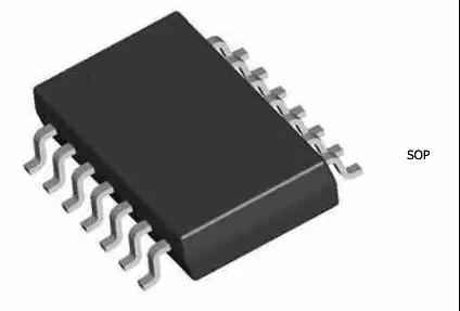
64、SOI(small out-line I-leaded package)
I-lead small outline package. One of the surface mount packages. The pins are led out from both sides of the package in an I-shape downwards, with a center distance of 1.27mm. The mounting area occupied is smaller than SOP. Hitachi uses this package in analog ICs (ICs for motor drives). Number of pins 26.
65、SOIC(small out-line integrated circuit)
Another name for SOP (see SOP). Many foreign semiconductor manufacturers use this name.
66、SOJ(Small Out-Line J-Leaded Package)
J-lead small outline package. One of the surface mount packages. The pins are drawn downward from both sides of the package in a J-shape, hence the name. Usually plastic products, most of them are used in memory LSI circuits such as DRAM and SRAM, but most of them are DRAM. Many DRAM devices packaged in SO J are assembled on SIMMs. The pin center distance is 1.27mm, and the number of pins ranges from 20 to 40 (see SIMM).
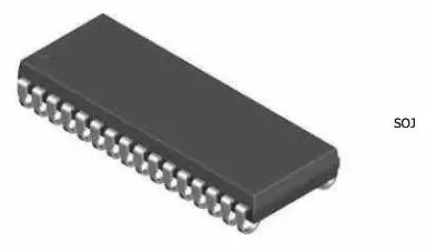
67、SQL(Small Out-Line L-leaded package)
The name adopted for SOP according to JEDEC (Joint Electronic Equipment Engineering Council) standard (see SOP).
68、SONF(Small Out-Line Non-Fin)
SOP without heat sink. Same as usual SOP. In order to indicate the difference in the power IC package without a heat sink, the NF (non-fin) mark is intentionally added. The name used by some semiconductor manufacturers (see SOP).
69、SOF(small Out-Line package)
Small form factor package. One of the surface mount packages, the pins are led out from both sides of the package in a gull wing shape (L shape). The materials are plastic and ceramic. Also called SOL and DFP.
In addition to being used in memory LSIs, SOPs are also widely used in circuits such as ASSPs that are not large in scale. In areas where the number of input and output terminals does not exceed 10 to 40, SOP is the most widely used surface mount package. The pin center distance is 1.27mm, and the number of pins is from 8 to 44.
In addition, SOPs with a pin center distance less than 1.27mm are also called SSOPs; SOPs with an assembly height of less than 1.27mm are also called TSOPs (see SSOP, TSOP). There is also an SOP with a heat sink.
70、SOW (Small Outline Package(Wide-Jype))
Wide body SOP. A name adopted by some semiconductor manufacturers.
—If there is any infringement, please contact us and delete it.
Company phone number: +86-0755-83044319
Fax/FAX: +86-0755-83975897
Email: 1615456225@qq.com
QQ: 3518641314 Manager Li
QQ: 332496225 Manager Qiu
Address: Room 809, Building C, Zhantao Technology Building, No. 1079 Minzhi Avenue, Longhua New District, Shenzhen
Related Recommendations
Exclusive Interview with Li Gang of Yunfan Ruida: The Precision of Millimeter-Wave Radar Products and the Warmth of Humanity
2026-07-22
2463
RF Passion, Craftsman’s Journey: Over 30 Years of Steadfast Dedication — Interview with Kinghelm Chief Engineer Mr. Qin hongxiang
2026-06-26
2644





 粤公网安备44030002007346号