
























Service Hotline
News

News
Diamond semiconductor? A comprehensive review of useful knowledge and scientific research teams!
2022-03-16
1194
Speaking of diamond, I think many people in life are not familiar with it. The editor has not entered this industry, and my understanding of diamond is limited to its perfect structure (PS the editor is a professional in fluorescent ceramic materials)…Might as well change the word "diamond", which is deeply rooted in people's hearts, BlingBling, full of temptation.
The century-old scam of "diamonds are forever" has buried the talent of diamonds and overskilled them. You think he is a rich man, but in fact he is a king.The application volume of diamond in the industrial field is much larger than that in the jewelry field. Especially in the future high-precision fields, diamond materials have great potential.
In the post-Moore era, the development of carbon-based electronics has received widespread attention. In the field of nanoelectronics, significant progress has been made in carbon-based nanoelectronics research, mainly one-dimensional carbon nanotubes and two-dimensional graphene.In the field of power electronics, research on diamond power electronics, which is known for ending semiconductors, is also showing great vitality, showing its potential to become the next generation of power electronics.
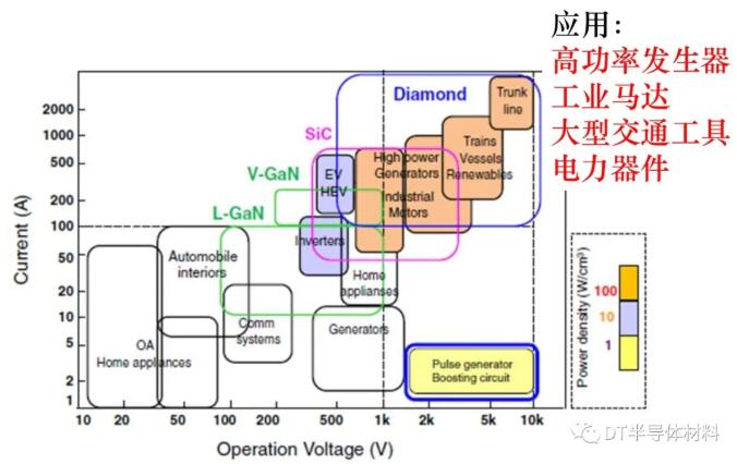
There is a reason why diamond semiconductor is hailed as the ultimate semiconductor by the industry. The current main research focus is based on the properties of diamond itself. (Picture from Carbontech 2020 report PPT by Professor Zhang Jinfeng of Xi'an University of Electronic Science and Technology)
Diamond is an ultra-wide bandgap semiconductor material with a bandgap width of 5.5 eV, which is larger than wide bandgap semiconductor materials such as GaN and SiC. As shown in the table below, the bandgap width of diamond is 5 times that of Si; the carrier mobility is also 3 times that of Si material. Theoretically, the carrier mobility of diamond is more than 2 times higher than existing wide bandgap semiconductor materials (GaN, SiC). At the same time, diamond has an extremely low intrinsic carrier concentration at room temperature. Moreover, in addition to the highest hardness, diamond also has the highest thermal conductivity among semiconductor materials, which is 7.5 times that of AlN. Based on these excellent performance parameters, diamond is considered to be the most promising material for preparing the next generation of high-power, high-frequency, high-temperature and low-power loss electronic devices, and is hailed as the "ultimate semiconductor" by the industry.
In particular, the 5G communication era is rapidly unfolding, and the application of diamond single crystal materials in semiconductors and high-frequency power devices has become increasingly prominent. Diamond single crystal and products are an important material basis for the implementation of major national strategies such as ultra-precision processing and smart grids, and the upgrading of industrial groups such as intelligent manufacturing and 5G communications. The breakthrough and industrialization of this technology are of great significance to the independent security of China's intelligent manufacturing and big data industries.
to this end, Research directions requiring diamond materialsLarge size, low defects, low resistivity and high thermal conductivitydirection of development。
Current research on diamond semiconductor materials and devices mainly focuses on the following aspects:
● Growth and equipment for large-size, high-quality diamonds
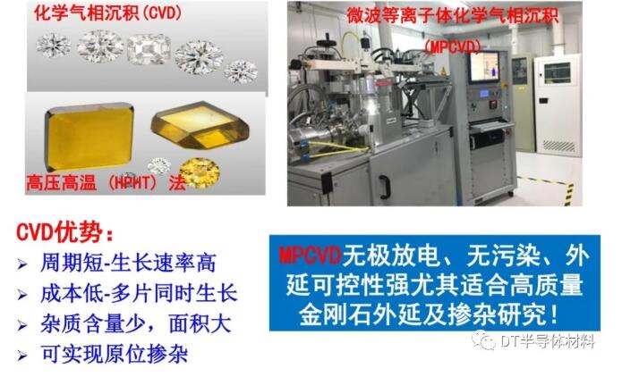
The preparation methods of diamond are mainly divided into high temperature and high pressure method (HPHT) and plasma chemical vapor deposition method (PCVD). Compared with HPHT method and other PCVD methods,MPCVD is electrodeless discharge, pollution-free, and has strong epitaxial controllability. It has more obvious advantages in large-size, high-purity diamond preparation and doping research. It is the preferred method for high-quality and multi-field application diamond preparation.。
Process and equipment
In terms of key technology development and marketization of advanced MPCVD equipment, teams from Japan, the United States, Germany and other countries are in a leading position. Among them, in the development and application of flat quartz window-type MPCVD equipment and CAP-type MPCVD equipment, Japan's Seki Company occupies the leading position in the world and maintains technological leadership. In terms of the development and application of quartz bell-type MPCVD equipment, the Asmussen team at Michigan State University in the United States developed a high-pressure (>2.4×10⁴Pa) works in a high-power-density microwave plasma resonant cavity to achieve high-speed deposition of diamond.
In terms of the development and application of quartz ring MPCVD devices, the MPCVD produced by Plassys of France and iPlas of Germany is very representative. Among them, iPlas equipment has a microwave slit coupling structure and is suitable for the preparation of large-size diamonds, but the deposition rate is not particularly ideal. In the research and development of ellipsoidal resonant cavity MPCVD equipment, Germany's Fraunhofer Institute and Aixtron have always maintained the world's top level. Compared with quartz bell type or quartz ring type MPCVD equipment, equipment with this structure is suitable for matching microwave power sources with higher power levels, which is beneficial to obtaining a larger area of plasma.Obtaining uniform, stable, and large-area microwave plasma is the ultimate goal of MPCVD equipment developers.
In recent years, domestic research teams related to MPCVD equipment development have achieved certain results in the development of new MPCVD resonant cavities. However, compared with advanced foreign teams, few domestic companies or institutions have broken through the technical difficulties of achieving large-scale commercial mass production. therefore,Breakthroughs in key technologies such as the independent optimized design of microwave plasma resonators and the improvement of large-size diamond preparation processes urgently require continued investment and research by relevant domestic teams. There is still a long way to explore in the future.
Diamond Polycrystalline and Applications
As a semiconductor material, the preparation requirements and application directions of diamond single crystal and polycrystalline materials are quite different.
Preparation method of CVD polycrystalline diamond film, includingHigh-power DC arc plasma jet CVD, hot wire CVD and MPCVD, etc.. The preparation of optical-grade and electronic-grade polycrystalline diamond films requires an ideal deposition rate and extremely low or controllable defect density. MPCVD without electrode contamination discharge will inevitably become an ideal method for the preparation of electronic-grade and optical-grade diamond films. However, the growth rate of polycrystalline diamond is slow, and its crystal orientation consistency is crucial for processing, making it difficult to process.
Currently, Element Six has achieved commercial mass production of 4-inch electronic-grade polycrystalline diamond. Li Chengming's team from the University of Science and Technology Beijing, Wang Jianhua's team from Wuhan University of Technology, and Yu Shengwang's team from Taiyuan University of Technology have all achieved certain results in the research on MPCVD preparation of optical-grade polycrystalline diamond films. Although there is still a gap between domestic optical grade and electronic grade polycrystalline diamond films and the international advanced level, the optical grade polycrystalline diamond films developed by domestic and above teams can meet the needs of infrared/radar dual-mode guidance windows, high-power CO2Basic application requirements for laser processing machine windows and high-power microwave windows.
Compared with the harsh preparation and application conditions of optical-grade and electronic-grade polycrystalline diamond films, polycrystalline diamond films are more widely used as heat sinks for heat dissipation of semiconductor power devices, and the demand is greater and more urgent. The current technical level of its precipitation is also relatively easy to achieve.
In addition, the manufacturing cost advantage of polycrystalline diamond is more obvious than that of single crystal diamond. In the past 30 years, research on the application of MPCVD polycrystalline diamond films as heat sinks in semiconductor devices has never stopped. Currently, inch-scale Si-based polycrystalline diamond films are used in HEMTs devices, and the RF power density of the devices has been effectively improved, reaching more than 23W/mm. Currently, the size of the prepared heat sink-grade polycrystalline diamond film can reach 8 inches. With the improvement and upgrade of MPCVD technology, it is expected to be compatible with the existing 8-inch semiconductor wafer manufacturing production line, ultimately realizing the large-scale application and promotion of polycrystalline diamond heat sink materials in the semiconductor material industry.
Diamond single crystal and applications
Compared with polycrystalline diamond, single crystal diamond (SCD) without grain boundary constraints has better optical and electrical properties. It has outstanding application effects in cutting-edge scientific and technological fields such as quantum communication/computing radiation detectors, cold cathode field emission displays, semiconductor lasers, supercomputer CPU chip multi-dimensional integrated circuits, and military high-power radar microwave traveling wave tube thermal conductive support rods. Preparing large-sized and high-quality SCD is a prerequisite.
As a diamond wafer, its size must be more than 2 inches. At present, the main technologies for preparing large-size diamonds and wafers areHomoepitaxial growth, mosaic wafer preparation and heteroepitaxial growthand other technologies.
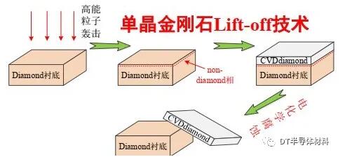
Mosaic splicing methodAs a highly feasible method for preparing large-size SCDs, the splicing and growth of multiple uniform substrates, combined with lift-off technology, has enabled the preparation of large-size SCDs. At present, single crystal wafers up to 2 inches have been achieved. However, high uniformity requirements for the substrate and the existence of grain boundaries will lead to problems such as stress and defects at the splicing joint, which affects the quality of the SCD spliced sheets. In addition, the cost is high, peeling technology needs to be injected, and the yield is very low. (Picture from Carbontech 2020 report PPT by Professor Zhang Jinfeng of Xi'an University of Electronic Science and Technology)
Synthesize high-qualityhomoepitaxialDiamond layer is one of the important technologies for preparing diamond electronic devices. It has the characteristics of low defect density and the maximum size can reach 0.5 inches (1 inch = 2.54 cm). In the process of homoepitaxial preparation of single crystal diamond, how to peel the single crystal diamond from the substrate is a very important link, and it is also relatively difficult. Because the substrate is also extremely hard single crystal diamond, it cannot be cut by ordinary cutting methods. Commonly used methods include mechanical polishing and laser cutting. (Picture from Carbontech 2020 report PPT by Professor Zhang Jinfeng of Xi'an University of Electronic Science and Technology)
In addition to homoepitaxial growth, heteroepitaxial growth is also an effective method for growing large-area single crystal diamond. Heteroepitaxy refers to the use of buffer layers on Si, sapphire, MgO and other substrates to alleviate the thermal mismatch and lattice mismatch between diamond and substrate, and ultimately achieve the growth of single crystal diamond films. The most effective buffer layer is Ir, etc. Theoretically, this method can grow single crystal diamond with a large enough area to meet its industrialization needs in the field of electronic devices. Its main disadvantage is the high defect density.
After breakthroughs in key technologies such as nitrogen addition high-speed growth, pulse discharge high-efficiency growth and ion implantation stripping in microwave plasma chemical vapor deposition (MPCVD) growth technology, multi-directional repetitive three-dimensional MPCVD high-speed epitaxial growth (growth rate 100 μm·h) has been achieved in the past 10 years.-1), innovative technologies such as the growth of large-sized, thick and polycrystalline diamond edges and the use of plasma CVD in (H, C, N, O) systems for 200 h without borders and continuous growth.
● P-type doping and N-type doping
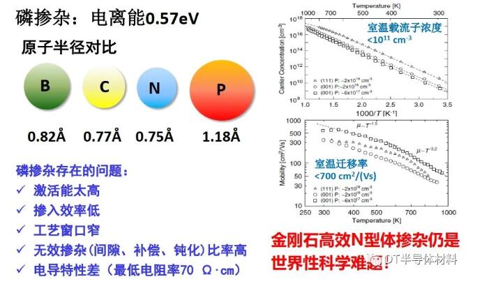
For diamond semiconductor devices, doping of diamond materials is the basic technology for forming power devices.The biggest problem in the commercialization of diamond semiconductors is that efficient bulk doping of diamond has not yet been solved. It is easy to manufacture P-type transistors but difficult to manufacture N-type transistors.。The p-type doping technology of diamond is relatively mature, and the main dopant is boron atoms. For p-type diamond, boron impurities can be easily integrated into natural diamond and MPCVD diamond, and there is no crystal orientation problem, but the activation efficiency of boron at room temperature is less than 0.1%. The doping concentration and mobility of boron in diamond have a trade-off relationship. Excessive doping concentration often leads to a rapid decrease in mobility. When the boron doping concentration is 1019 cm-3, the mobility will be reduced to 100 cm2·V -1·s-1the following. (Picture from Carbontech 2020 report PPT by Professor Zhang Jinfeng of Xi'an University of Electronic Science and Technology)
Selected based on the position of diamond's C atom (covalent radius 0.077 nm) in the periodic table of elements, the closest one is nitrogen (N) atom (0.075 nm), which makes it also a favorable candidate for n-type doping of diamond. However, after doping, the N atoms that replace C atoms in diamond are distorted due to the Jahn-Teller effect, causing the local lattice to skew and the N atoms to deviate from the replaced position. Its doping energy level is very deep, 1.7 eV, making it difficult to conduct electricity at room temperature.
(Picture from Carbontech 2020 report PPT by Professor Zhang Jinfeng of Xi'an University of Electronic Science and Technology)
With the continuous development of diamond semiconductor technology, bottlenecks such as n-type doping technology, large-size and high-quality single crystal preparation, and high-flatness and high-uniformity material epitaxy technology will surely be broken through in the future to realize diamond electronic devices with higher power performance. But this is inseparable from the unremitting efforts of scientific researchers!
●Ultrawide Bandgap Semiconductor Diamond Power Electronics
power diode: In the past 10 years, the progress of CVD diamond materials in terms of large size, low defects and heavy doping has directly driven the development of diamond diodes in the direction of high breakdown voltage, high breakdown field strength, low on-resistance, high switching rate and high-temperature operation. Both types of SBD and p-n junction diodes are under development, among which diamond SBD is developing faster and is already in the preliminary application experimental stage.
The main reason for the low breakdown voltage of diamond diodes and transistors (less than 500 V) is the difficulty in controlling the doping substances in diamond. Diamond is the material with the highest atomic density on earth. Except for a few small atoms such as H, P, N and Si elements, it is difficult to add other large atoms into its crystal.
Diamond p-i-n diodeis an advanced device suitable for high-power applications, except that its critical electric field is 3 MV·cm-1(SiC theoretical limit), the series resistance of diamond p-i-n diodes can also be significantly reduced by using a heavily doped layer. In the past 10 years, diamond p-i-n diode technology has made great progress, such as breakthroughs in the preparation of heavily doped p+ and n+ layers with transition conduction mechanisms; carrier transport mechanisms of diamond p+-i-n+ junction diodes with low resistance transition conductivity; material structure optimization design of Schottky diamond p-n diodes (SPND); selective growth of n+ Research on the mechanism of the impact of interface defects of layers and p-n junction diodes on reverse leakage; research on reverse recovery and minority carrier lifetime of diamond p-i-n diodes; research on the mechanism of uneven Schottky barrier height of diamond Schottky p-i-n diodes (SPIND) and other key technologies.
Power transistors and logic circuits
Diamond transistors have made progress in both the fields of power electronics and microwave electronics. In the field of power electronics, the development direction is towards high breakdown voltage, high breakdown field strength, high temperature operation, low on-resistance, high switching rate and normally-off devices.Diamond transistors are mainly composed of various types of FETs, includingMetal Semiconductor Field Effect Transistors (MESFETs), MOSFETs and JFETsetc. There are two types of channels: diamond hydrogen terminal surface two-dimensional hole gas and p-type doped layer. With the advancement of n-type doping materials, bipolar diamond devices have begun to appear, and recently heterojunction bipolar transistors have been developed. In the field of microwave electronics, hydrogen-terminated FETs are dominant and are developing towards high fT/fmax and high power density.
Diamond MESFET uses Schottky barrier to modulate and control the channel. Technological advances in recent years include: combination of wide gate-drain spacing and lightly doped p-channel, research on the effect of reduced gate-source spacing, passing 14.8 MeV neutron irradiation experiments, higher boron doping concentration and good surface epitaxial channel layer technology, and high-temperature annealing of boron-doped diamond MESFET.
Diamond MOSFETIt is the most widely studied diamond transistor, which uses a MOS gate control structure to suppress gate leakage current. In recent years, diamond MOSFFT has been dominated by hydrogen-terminated channel devices and has made breakthroughs in a series of key technologies such as the highly stable Al2O3 gate oxide layer structure.
For applications of power devices operating at high voltages and high temperatures, the diamond body channel device JFET, which is more stable than surface channel devices, is more advantageous.
Diamond BJTIt is one of the main power switching devices. Compared with hydrogen-terminated diamond FETs, diamond-based BJTs have no gate dielectric layer, hydrogen-terminated surface conductivity, and conductance modulation effects that can achieve minority carrier injection, resulting in potentially lower on-resistance. A key parameter of power BJTs is the amplification factor of the common emitter current, which enables current amplification compared to diamond FETs to reduce the power requirements of the drive circuit.
diamond logic circuit: The development of diamond logic circuits is the first step in the development of diamond ICs. With the development of enhanced diamond MISFETs, the research and development of diamond logic circuits has been driven.
RF FET: Diamond has semiconductor properties such as high thermal conductivity, high breakdown field strength and high carrier saturation velocity. For this reason, diamond high-frequency and high-power devices are also one of the research hotspots of diamond electronics.
GaN on diamond HEMT:The covalent bonds between diamond atoms are extremely strong, giving the rigid structure a high vibration frequency. Its Debye characteristic temperature is as high as 2200 K. The phonon scattering is small, so the resistance to heat conduction using phonons as a medium is extremely small. Its thermal conductivity is five times that of copper, up to 2000 W/(m·K). Wide-bandgap semiconductor GaN microwave electronics has become the current mainstream after nearly two decades of development, and its thermal management issues have become the main obstacle to its further development. Therefore, the combination of the thermal conductivity advantages of ultra-wide-bandgap diamond and GaN technology has become inevitable for the development of the next generation of GaN microwave electronics. It also provides a basis for the ongoing development of GaN microwave electronics.2O3Provide reference for thermal management of electronic devices, etc. Diamond materials can be used as thermal management materials for power electronic devices, and are developing in the direction of large size, low interface thermal resistance, and high thermal conductivity.
。。。
● Heat dissipation components and applications
With the widespread application of third-generation semiconductors and the advent of the 5G era, traditional electronic packaging thermal management materials and even chip materials are facing huge challenges in upgrading. Advanced carbon and its composite materials, which have emerged rapidly in recent years, will play an important role in the field of heat dissipation of high-power, high-frequency optoelectronic devices and become ideal thermal management materials in the electronics industry! (Including heat sink materials, packaging materials, base materials, etc.). (Picture from Carbontech 2020 report PPT by Professor Wang Chengyong of Guangdong University of Technology)
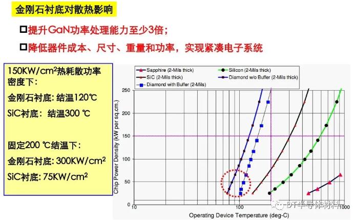
Diamond heat dissipation substrate in GaN-based power devices:The full performance of gallium nitride (GaN)-based power devices is limited by the low thermal conductivity of the substrate on which GaN is deposited. Chemical vapor deposition (CVD) diamond with high thermal conductivity has become an excellent choice for thermal diffusion substrate materials for GaN power devices. Relevant scholars have carried out a number of technical studies on the combination of high thermal conductivity diamond and GaN devices, mainly including low-temperature bonding technology, substrate transfer technology for directly growing diamond on the back of the GaN epitaxial layer, single crystal diamond epitaxial GaN technology and high thermal conductivity diamond passivation layer heat dissipation technology.
Directly growing diamond on the back of the GaN epitaxial layer has good interface bonding strength, but involves technical difficulties such as high temperature, high wafer stress, and high interface thermal resistance. Single crystal diamond epitaxial GaN technology and high thermal conductivity diamond passivation layer heat dissipation technology are respectively limited by the small size, high cost and process incompatibility of single crystal diamond. Therefore, developing low-cost large-size diamond substrates, improving wafer stress control technology and interface bonding strength, reducing interface thermal resistance, and improving the performance of diamond substrate GaN devices will be the focus of future development of diamond and GaN device bonding technology.
(Picture from Carbontech 2020 report PPT by Professor Zhang Jinfeng of Xi'an University of Electronic Science and Technology)
Diamond packaged semiconductor laser
When a high-power semiconductor laser is working, the active area will generate a large amount of heat, which will reduce the output power of the laser and shorten its service life. Diamond has high thermal conductivity characteristics. Using it as a transition heat sink will improve the heat dissipation capacity of the device, reduce thermal resistance, increase laser output power, and extend laser life.
Diamond Raman Laser Research:Stimulated Raman scattering is an important nonlinear optical effect. Stimulated Raman scattering can achieve a fixed frequency displacement of all incident photons without the need for phase matching. It is an important technology for expanding the use band range of lasers. Research in this direction has become a hot spot in the development of laser technology.
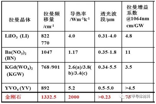
As a crystal Raman material with excellent performance, diamond has the largest Raman frequency shift of 1332.3 cm among known crystal materials.-1, its Raman gain linewidth is about 1.5 cm at room temperature-1. The Raman gain of diamond has polarization selectivity. When the polarization direction of the pump light is parallel to the <111> direction of the diamond crystal, its Raman gain is maximum (10 cm/GW@1 μm), and linearly polarized Raman light is output. Diamond has ultra-high thermal conductivity, and its ultra-fast heat dissipation ability is the key for diamond crystals to maintain high Raman gain and obtain high-beam quality laser output under high-power operation.
Comparison between common laser Raman crystals and diamond
In recent years, with the improvement of chemical vapor deposition preparation technology, the optical quality of artificial diamond has been rapidly improved. Optical-grade diamond crystals have also shown excellent power improvement, coherence enhancement and frequency conversion capabilities with their excellent Raman and Brillouin characteristics. This has promoted diamond lasers to greatly overcome the thermal effects of particle number inversion lasers based on traditional working materials, as well as the difficulty of balancing wavelength and output power.
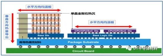
Single crystal diamond 3D packaging heat dissipation substrate:
When following Moore's Law has become an industry consensus, the proposal of More Moore seems to have added some brightness to the development of the chip manufacturing industry. Generally speaking, More Moore refers to the continuous shrinking of chip feature sizes, which includes two aspects: continuing to shrink the feature size in the horizontal and vertical directions of the wafer in order to improve density, performance and reliability; using process technologies such as 3D structures and the use of new materials to affect the electrical performance of the wafer. (Picture from Carbontech 2020 report PPT by Jiangnan researcher at Ningbo Institute of Materials)
Electronic packaging materials are used to carry electronic components and their interconnections. They mainly serve as mechanical support, sealing protection, heat dissipation and shielding. They have a very important impact on the performance and reliability of integrated circuits. With the development of electronic technology, integrated circuits are developing towards ultra-large scale, ultra-high speed, high density, high power, high precision, and multi-function, which places higher and higher requirements on packaging materials. The research and development of multi-system high-performance packaging materials such as diamond/copper, diamond/aluminum, diamond/silicon carbide, graphite/copper, etc. is of great significance in promoting the development of electronic packaging materials in the direction of miniaturization, high performance, high reliability and low cost.
。。。。。
●Ultra-precision machining
Diamond materials and laser processing technology:Compared with other materials, diamond has the characteristics of high resistivity, high breakdown field strength, low dielectric constant, and low thermal expansion. Its application in thermal management can meet the requirements of high-density and highly integrated assembly development in the rapidly developing electronics industry. Laser processing can achieve high-quality processing of diamond microstructures. It is an advanced manufacturing technology that is currently being researched at home and abroad.
Diamond substrate grinding and polishing technology
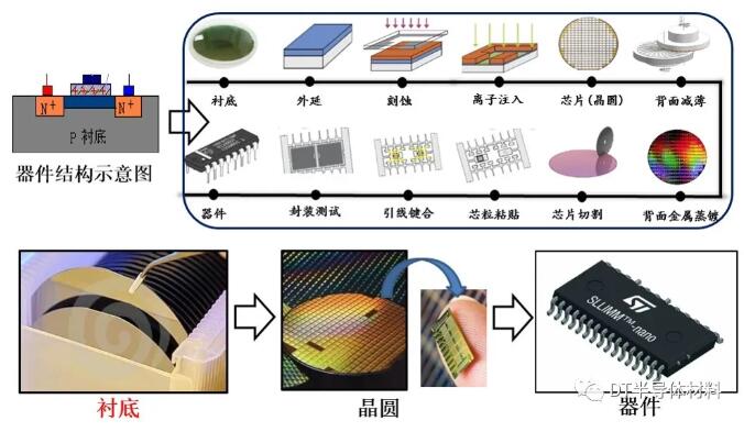
Semiconductor devices mainly include integrated circuits, power devices, optoelectronic devices and sensors, etc. Power devices are widely used in aerospace, military and national defense, power energy, rail transportation, and information Internet of Things. The semiconductor wafer is the carrier of the semiconductor device, and the semiconductor substrate is the carrier of the semiconductor wafer. The substrate is the epitaxial base of semiconductor devices, which directly determines the quality and performance of the device.
Ultra-precision machining
The objects of ultra-precision machining are generally small-sized diamond materials, which are too costly for industrialization and are not conducive to industrial application. To successfully apply diamond to the heat dissipation of power devices and achieve industrialization, the acquisition of large-size wafer-level heat dissipation base materials with good surface quality is a key. In addition, as the level of circuit integration on diamond substrates increases, the requirements for surface quality will gradually increase. Surface roughness will develop to the angstrom level or even smaller, and surface warpage will reach 5 μm or smaller.
Disclaimer: This article is reproduced from "DT Semiconductor Materials", which supports the protection of intellectual property rights. Please indicate the original source and author of the reprint. If there is any infringement, please contact us to delete it.

Related Recommendations
Exclusive Interview with Li Gang of Yunfan Ruida: The Precision of Millimeter-Wave Radar Products and the Warmth of Humanity
2026-07-22
2517
RF Passion, Craftsman’s Journey: Over 30 Years of Steadfast Dedication — Interview with Kinghelm Chief Engineer Mr. Qin hongxiang
2026-06-26
2687





 粤公网安备44030002007346号