
























Service-Hotline
Nachrichten

Nachrichten
Diamant-Halbleiter? Ein umfassender Überblick über nützliches Wissen und wissenschaftliche Forschungsteams!
2022-03-16
1193
Apropos Diamanten: Ich glaube, vielen Menschen ist dieser Begriff nicht geläufig. Der/Die Redakteur/in ist nicht in dieser Branche tätig, und mein Wissen über Diamanten beschränkt sich auf deren perfekte Struktur (PS: Der/Die Redakteur/in ist Experte/Expertin für fluoreszierende Keramikmaterialien)....Man könnte genauso gut das Wort „Diamant“ ändern, das tief in den Herzen der Menschen verwurzelt ist, BlingBling, voller Versuchung.
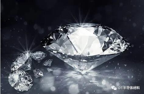
The century-old scam of "diamonds are forever" has buried the talent of diamonds and overskilled them. You think he is a rich man, but in fact he is a king.Das Anwendungsvolumen von Diamanten im industriellen Bereich ist wesentlich größer als im Schmuckbereich.. Especially in the future high-precision fields, diamond materials have great potential.
In the post-Moore era, the development of carbon-based electronics has received widespread attention. In the field of nanoelectronics, significant progress has been made in carbon-based nanoelectronics research, mainly one-dimensional carbon nanotubes and two-dimensional graphene.In the field of power electronics, research on diamond power electronics, which is known for ending semiconductors, is also showing great vitality, showing its potential to become the next generation of power electronics.
There is a reason why diamond semiconductor is hailed as the ultimate semiconductor by the industry. The current main research focus is based on the properties of diamond itself.
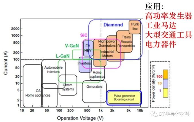
(Picture from Carbontech 2020 report PPT by Professor Zhang Jinfeng of Xi'an University of Electronic Science and Technology)
Diamond is an ultra-wide bandgap semiconductor material with a bandgap width of 5.5 eV, which is larger than wide bandgap semiconductor materials such as GaN and SiC. As shown in the table below, the bandgap width of diamond is 5 times that of Si; the carrier mobility is also 3 times that of Si material. Theoretically, the carrier mobility of diamond is more than 2 times higher than existing wide bandgap semiconductor materials (GaN, SiC). At the same time, diamond has an extremely low intrinsic carrier concentration at room temperature. Moreover, in addition to the highest hardness, diamond also has the highest thermal conductivity among semiconductor materials, which is 7.5 times that of AlN. Based on these excellent performance parameters, diamond is considered to be the most promising material for preparing the next generation of high-power, high-frequency, high-temperature and low-power loss electronic devices, and is hailed as the "ultimate semiconductor" by the industry.
In particular, the 5G communication era is rapidly unfolding, and the application of diamond single crystal materials in semiconductors and high-frequency power devices has become increasingly prominent. Diamond single crystal and products are an important material basis for the implementation of major national strategies such as ultra-precision processing and smart grids, and the upgrading of industrial groups such as intelligent manufacturing and 5G communications. The breakthrough and industrialization of this technology are of great significance to the independent security of China's intelligent manufacturing and big data industries.
to this end, Research directions requiring diamond materialsLarge size, low defects, low resistivity and high thermal conductivitydirection of development.
Current research on diamond semiconductor materials and devices mainly focuses on the following aspects:
● Anbau und Ausrüstung für große, hochwertige Diamanten
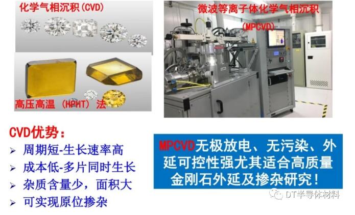
The preparation methods of diamond are mainly divided into high temperature and high pressure method (HPHT) and plasma chemical vapor deposition method (PCVD). Compared with HPHT method and other PCVD methods,MPCVD is electrodeless discharge, pollution-free, and has strong epitaxial controllability. It has more obvious advantages in large-size, high-purity diamond preparation and doping research. It is the preferred method for high-quality and multi-field application diamond preparation..
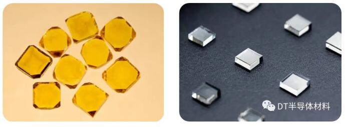
Prozess und Ausrüstung
Im Bereich der Schlüsseltechnologieentwicklung und Markteinführung fortschrittlicher MPCVD-Anlagen nehmen Teams aus Japan, den USA, Deutschland und anderen Ländern eine führende Position ein. Insbesondere bei der Entwicklung und Anwendung von MPCVD-Anlagen mit flachem Quarzfenster und CAP-MPCVD-Anlagen ist das japanische Unternehmen Seki weltweit führend und behauptet seine Technologieführerschaft. Im Bereich der Entwicklung und Anwendung von MPCVD-Anlagen mit Quarzglocke entwickelte das Team von Asmussen an der Michigan State University in den USA eine Hochdruckanlage (>2.4 × 10⁶ mbar).4Pa) arbeitet in einem Mikrowellenplasma-Resonator mit hoher Leistungsdichte, um eine Hochgeschwindigkeitsabscheidung von Diamant zu erreichen.
In terms of the development and application of quartz ring MPCVD devices, the MPCVD produced by Plassys of France and iPlas of Germany is very representative. Among them, iPlas equipment has a microwave slit coupling structure and is suitable for the preparation of large-size diamonds, but the deposition rate is not particularly ideal. In the research and development of ellipsoidal resonant cavity MPCVD equipment, Germany's Fraunhofer Institute and Aixtron have always maintained the world's top level. Compared with quartz bell type or quartz ring type MPCVD equipment, equipment with this structure is suitable for matching microwave power sources with higher power levels, which is beneficial to obtaining a larger area of plasma.Die Erzeugung eines gleichmäßigen, stabilen und großflächigen Mikrowellenplasmas ist das oberste Ziel der Entwickler von MPCVD-Anlagen.
In den letzten Jahren haben inländische Forschungsteams im Bereich der MPCVD-Anlagenentwicklung gewisse Erfolge bei der Entwicklung neuer MPCVD-Resonatoren erzielt. Im Vergleich zu fortgeschrittenen ausländischen Teams ist es jedoch nur wenigen inländischen Unternehmen oder Institutionen gelungen, die technischen Hürden für eine groß angelegte kommerzielle Massenproduktion zu überwinden.Bahnbrechende Fortschritte bei Schlüsseltechnologien wie der unabhängigen Optimierung von Mikrowellenplasmaresonatoren und der Verbesserung von Verfahren zur Herstellung großformatiger Diamanten erfordern dringend weitere Investitionen und Forschung durch entsprechende inländische Teams. Es gibt noch viel zu entdecken.
Diamond Polycrystalline and Applications
As a semiconductor material, the preparation requirements and application directions of diamond single crystal and polycrystalline materials are quite different.
Herstellungsverfahren für polykristalline CVD-Diamantschichten, einschließlichHigh-power DC arc plasma jet CVD, hot wire CVD and MPCVD, etc.. The preparation of optical-grade and electronic-grade polycrystalline diamond films requires an ideal deposition rate and extremely low or controllable defect density. MPCVD without electrode contamination discharge will inevitably become an ideal method for the preparation of electronic-grade and optical-grade diamond films. However, the growth rate of polycrystalline diamond is slow, and its crystal orientation consistency is crucial for processing, making it difficult to process.
Currently, Element Six has achieved commercial mass production of 4-inch electronic-grade polycrystalline diamond. Li Chengming's team from the University of Science and Technology Beijing, Wang Jianhua's team from Wuhan University of Technology, and Yu Shengwang's team from Taiyuan University of Technology have all achieved certain results in the research on MPCVD preparation of optical-grade polycrystalline diamond films. Although there is still a gap between domestic optical grade and electronic grade polycrystalline diamond films and the international advanced level, the optical grade polycrystalline diamond films developed by domestic and above teams can meet the needs of infrared/radar dual-mode guidance windows, high-power CO2Basic application requirements for laser processing machine windows and high-power microwave windows.
Compared with the harsh preparation and application conditions of optical-grade and electronic-grade polycrystalline diamond films, polycrystalline diamond films are more widely used as heat sinks for heat dissipation of semiconductor power devices, and the demand is greater and more urgent. The current technical level of its precipitation is also relatively easy to achieve.
In addition, the manufacturing cost advantage of polycrystalline diamond is more obvious than that of single crystal diamond. In the past 30 years, research on the application of MPCVD polycrystalline diamond films as heat sinks in semiconductor devices has never stopped. Currently, inch-scale Si-based polycrystalline diamond films are used in HEMTs devices, and the RF power density of the devices has been effectively improved, reaching more than 23W/mm. Currently, the size of the prepared heat sink-grade polycrystalline diamond film can reach 8 inches. With the improvement and upgrade of MPCVD technology, it is expected to be compatible with the existing 8-inch semiconductor wafer manufacturing production line, ultimately realizing the large-scale application and promotion of polycrystalline diamond heat sink materials in the semiconductor material industry.
Diamant-Einkristall und seine Anwendungen
Compared with polycrystalline diamond, single crystal diamond (SCD) without grain boundary constraints has better optical and electrical properties. It has outstanding application effects in cutting-edge scientific and technological fields such as quantum communication/computing radiation detectors, cold cathode field emission displays, semiconductor lasers, supercomputer CPU chip multi-dimensional integrated circuits, and military high-power radar microwave traveling wave tube thermal conductive support rods. Preparing large-sized and high-quality SCD is a prerequisite.
As a diamond wafer, its size must be more than 2 inches. At present, the main technologies for preparing large-size diamonds and wafers areHomoepitaxial growth, mosaic wafer preparation and heteroepitaxial growthund andere Technologien.
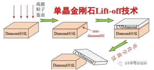
Mosaik-SpleißmethodeAs a highly feasible method for preparing large-size SCDs, the splicing and growth of multiple uniform substrates, combined with lift-off technology, has enabled the preparation of large-size SCDs. At present, single crystal wafers up to 2 inches have been achieved. However, high uniformity requirements for the substrate and the existence of grain boundaries will lead to problems such as stress and defects at the splicing joint, which affects the quality of the SCD spliced sheets. In addition, the cost is high, peeling technology needs to be injected, and the yield is very low.
(Picture from Carbontech 2020 report PPT by Professor Zhang Jinfeng of Xi'an University of Electronic Science and Technology)
Synthesize high-qualityhomoepitaxialDie Diamantschicht ist eine wichtige Technologie zur Herstellung diamantbasierter elektronischer Bauelemente. Sie zeichnet sich durch eine geringe Defektdichte aus und kann eine maximale Größe von 0.5 Zoll (1 Zoll = 2.54 cm) erreichen. Bei der homoepitaktischen Herstellung von Einkristalldiamanten ist das Ablösen der Einkristalle vom Substrat ein entscheidender und zugleich schwieriger Schritt. Da das Substrat ebenfalls aus extrem hartem Einkristalldiamanten besteht, kann es nicht mit herkömmlichen Schneidverfahren bearbeitet werden. Gängige Methoden sind das mechanische Polieren und das Laserschneiden.
(Picture from Carbontech 2020 report PPT by Professor Zhang Jinfeng of Xi'an University of Electronic Science and Technology)
In addition to homoepitaxial growth, heteroepitaxial growth is also an effective method for growing large-area single crystal diamond. Heteroepitaxy refers to the use of buffer layers on Si, sapphire, MgO and other substrates to alleviate the thermal mismatch and lattice mismatch between diamond and substrate, and ultimately achieve the growth of single crystal diamond films. The most effective buffer layer is Ir, etc. Theoretically, this method can grow single crystal diamond with a large enough area to meet its industrialization needs in the field of electronic devices. Its main disadvantage is the high defect density.
After breakthroughs in key technologies such as nitrogen addition high-speed growth, pulse discharge high-efficiency growth and ion implantation stripping in microwave plasma chemical vapor deposition (MPCVD) growth technology, multi-directional repetitive three-dimensional MPCVD high-speed epitaxial growth (growth rate 100 μm·h) has been achieved in the past 10 years.-1), innovative technologies such as the growth of large-sized, thick and polycrystalline diamond edges and the use of plasma CVD in (H, C, N, O) systems for 200 h without borders and continuous growth.
● P-type doping and N-type doping

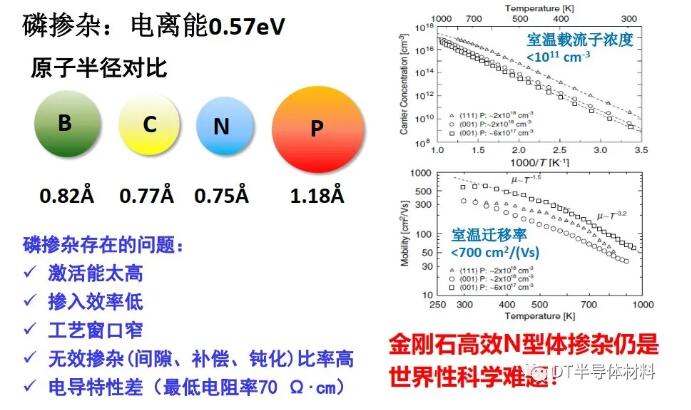
For diamond semiconductor devices, doping of diamond materials is the basic technology for forming power devices.The biggest problem in the commercialization of diamond semiconductors is that efficient bulk doping of diamond has not yet been solved. It is easy to manufacture P-type transistors but difficult to manufacture N-type transistors..Die p-Dotierungstechnologie von Diamant ist relativ ausgereift, wobei Boratome das Hauptdotiermittel sind. Bei p-Diamant lassen sich Borverunreinigungen leicht in natürlichen Diamanten und MPCVD-Diamanten integrieren, ohne dass Probleme mit der Kristallorientierung auftreten. Die Aktivierungseffizienz von Bor bei Raumtemperatur liegt jedoch unter 0.1 %. Zwischen Dotierungskonzentration und Mobilität von Bor in Diamant besteht ein Zielkonflikt. Eine zu hohe Dotierungskonzentration führt häufig zu einem raschen Abfall der Mobilität. Bei einer Bor-Dotierungskonzentration von 1019 cm-3Die Mobilität wird auf 100 cm reduziert.2·V -1· S.-1folgende.
(Picture from Carbontech 2020 report PPT by Professor Zhang Jinfeng of Xi'an University of Electronic Science and Technology)
Selected based on the position of diamond's C atom (covalent radius 0.077 nm) in the periodic table of elements, the closest one is nitrogen (N) atom (0.075 nm), which makes it also a favorable candidate for n-type doping of diamond. However, after doping, the N atoms that replace C atoms in diamond are distorted due to the Jahn-Teller effect, causing the local lattice to skew and the N atoms to deviate from the replaced position. Its doping energy level is very deep, 1.7 eV, making it difficult to conduct electricity at room temperature.
(Picture from Carbontech 2020 report PPT by Professor Zhang Jinfeng of Xi'an University of Electronic Science and Technology)
With the continuous development of diamond semiconductor technology, bottlenecks such as n-type doping technology, large-size and high-quality single crystal preparation, and high-flatness and high-uniformity material epitaxy technology will surely be broken through in the future to realize diamond electronic devices with higher power performance. But this is inseparable from the unremitting efforts of scientific researchers!
●Ultrabreitbandige Halbleiter-Diamant-Leistungselektronik
Leistungsdiode: In the past 10 years, the progress of CVD diamond materials in terms of large size, low defects and heavy doping has directly driven the development of diamond diodes in the direction of high breakdown voltage, high breakdown field strength, low on-resistance, high switching rate and high-temperature operation. Both types of SBD and p-n junction diodes are under development, among which diamond SBD is developing faster and is already in the preliminary application experimental stage.
The main reason for the low breakdown voltage of diamond diodes and transistors (less than 500 V) is the difficulty in controlling the doping substances in diamond. Diamond is the material with the highest atomic density on earth. Except for a few small atoms such as H, P, N and Si elements, it is difficult to add other large atoms into its crystal.
Diamond p-i-n diodeis an advanced device suitable for high-power applications, except that its critical electric field is 3 MV·cm-1(Theoretische Grenze von SiC) lässt sich der Serienwiderstand von Diamant-PIN-Dioden durch den Einsatz einer hochdotierten Schicht deutlich reduzieren. In den letzten zehn Jahren wurden in der Diamant-PIN-Dioden-Technologie große Fortschritte erzielt, darunter Durchbrüche bei der Herstellung hochdotierter p+- und n+-Schichten mit Übergangsleitmechanismen; Ladungstransportmechanismen von Diamant-p+-i-n+-Übergangsdioden mit niedrigem Übergangswiderstand; Optimierung der Materialstruktur von Schottky-Diamant-pn-Dioden (SPND); selektives Wachstum von n+-Schichten; Forschung zum Einfluss von Grenzflächendefekten in Schichten und pn-Übergangsdioden auf den Sperrstrom; Forschung zur Sperrverzögerung und Minoritätsträgerlebensdauer von Diamant-PIN-Dioden; Forschung zum Mechanismus der ungleichmäßigen Schottky-Barrierenhöhe von Diamant-Schottky-PIN-Dioden (SPIND) und andere Schlüsseltechnologien.
Power transistors and logic circuits
Diamond transistors have made progress in both the fields of power electronics and microwave electronics. In the field of power electronics, the development direction is towards high breakdown voltage, high breakdown field strength, high temperature operation, low on-resistance, high switching rate and normally-off devices.Diamanttransistoren bestehen hauptsächlich aus verschiedenen Arten von FETs, darunterMetall-Halbleiter-Feldeffekttransistoren (MESFETs), MOSFETs und JFETsetc. There are two types of channels: diamond hydrogen terminal surface two-dimensional hole gas and p-type doped layer. With the advancement of n-type doping materials, bipolar diamond devices have begun to appear, and recently heterojunction bipolar transistors have been developed. In the field of microwave electronics, hydrogen-terminated FETs are dominant and are developing towards high fT/fmax and high power density.
Diamant-MESFETs nutzen Schottky-Barrieren zur Modulation und Steuerung des Kanals. Zu den technologischen Fortschritten der letzten Jahre zählen: die Kombination aus großem Gate-Drain-Abstand und schwach dotiertem p-Kanal, die Erforschung des Effekts eines reduzierten Gate-Source-Abstands, das Bestehen von Neutronenbestrahlungsexperimenten mit 14.8 MeV, höhere Bor-Dotierungskonzentrationen und eine verbesserte Technologie für die epitaktische Oberflächenkanalschicht sowie das Hochtemperaturglühen von bor-dotierten Diamant-MESFETs.
Diamond MOSFETIt is the most widely studied diamond transistor, which uses a MOS gate control structure to suppress gate leakage current. In recent years, diamond MOSFFT has been dominated by hydrogen-terminated channel devices and has made breakthroughs in a series of key technologies such as the highly stable Al2O3 gate oxide layer structure.
For applications of power devices operating at high voltages and high temperatures, the diamond body channel device JFET, which is more stable than surface channel devices, is more advantageous.
Diamant BJTEs handelt sich um eines der wichtigsten Leistungsschaltbauelemente. Im Vergleich zu wasserstoffterminierten Diamant-FETs weisen diamantbasierte Bipolartransistoren (BJTs) keine Gate-Dielektrikumsschicht, keine wasserstoffterminierte Oberflächenleitfähigkeit und Leitwertmodulationseffekte auf, die eine Minoritätsträgerinjektion ermöglichen und somit potenziell einen geringeren Einschaltwiderstand zur Folge haben. Ein Schlüsselparameter von Leistungs-BJTs ist der Verstärkungsfaktor des Emitterstroms, der im Vergleich zu Diamant-FETs eine Stromverstärkung ermöglicht und dadurch den Leistungsbedarf der Ansteuerschaltung reduziert.
diamond logic circuitDie Entwicklung von Diamantlogikschaltungen ist der erste Schritt zur Entwicklung von Diamant-ICs. Mit der Entwicklung verbesserter Diamant-MISFETs wurde die Forschung und Entwicklung von Diamantlogikschaltungen vorangetrieben.
HF-FET: Diamond has semiconductor properties such as high thermal conductivity, high breakdown field strength and high carrier saturation velocity. For this reason, diamond high-frequency and high-power devices are also one of the research hotspots of diamond electronics.
GaN on diamond HEMT:The covalent bonds between diamond atoms are extremely strong, giving the rigid structure a high vibration frequency. Its Debye characteristic temperature is as high as 2200 K. The phonon scattering is small, so the resistance to heat conduction using phonons as a medium is extremely small. Its thermal conductivity is five times that of copper, up to 2000 W/(m·K). Wide-bandgap semiconductor GaN microwave electronics has become the current mainstream after nearly two decades of development, and its thermal management issues have become the main obstacle to its further development. Therefore, the combination of the thermal conductivity advantages of ultra-wide-bandgap diamond and GaN technology has become inevitable for the development of the next generation of GaN microwave electronics. It also provides a basis for the ongoing development of GaN microwave electronics.2O3Provide reference for thermal management of electronic devices, etc. Diamond materials can be used as thermal management materials for power electronic devices, and are developing in the direction of large size, low interface thermal resistance, and high thermal conductivity.
...
● Heat dissipation components and applications
With the widespread application of third-generation semiconductors and the advent of the 5G era, traditional electronic packaging thermal management materials and even chip materials are facing huge challenges in upgrading. Advanced carbon and its composite materials, which have emerged rapidly in recent years, will play an important role in the field of heat dissipation of high-power, high-frequency optoelectronic devices and become ideal thermal management materials in the electronics industry! (Including heat sink materials, packaging materials, base materials, etc.).
(Abbildung aus der Präsentation „Carbontech 2020“ von Professor Wang Chengyong von der Technischen Universität Guangdong)
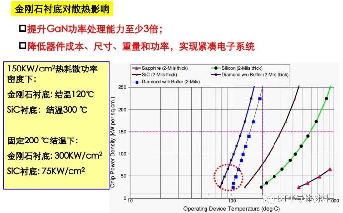
Diamond heat dissipation substrate in GaN-based power devices:The full performance of gallium nitride (GaN)-based power devices is limited by the low thermal conductivity of the substrate on which GaN is deposited. Chemical vapor deposition (CVD) diamond with high thermal conductivity has become an excellent choice for thermal diffusion substrate materials for GaN power devices. Relevant scholars have carried out a number of technical studies on the combination of high thermal conductivity diamond and GaN devices, mainly including low-temperature bonding technology, substrate transfer technology for directly growing diamond on the back of the GaN epitaxial layer, single crystal diamond epitaxial GaN technology and high thermal conductivity diamond passivation layer heat dissipation technology.
Directly growing diamond on the back of the GaN epitaxial layer has good interface bonding strength, but involves technical difficulties such as high temperature, high wafer stress, and high interface thermal resistance. Single crystal diamond epitaxial GaN technology and high thermal conductivity diamond passivation layer heat dissipation technology are respectively limited by the small size, high cost and process incompatibility of single crystal diamond. Therefore, developing low-cost large-size diamond substrates, improving wafer stress control technology and interface bonding strength, reducing interface thermal resistance, and improving the performance of diamond substrate GaN devices will be the focus of future development of diamond and GaN device bonding technology.
(Picture from Carbontech 2020 report PPT by Professor Zhang Jinfeng of Xi'an University of Electronic Science and Technology)
Diamond packaged semiconductor laser
When a high-power semiconductor laser is working, the active area will generate a large amount of heat, which will reduce the output power of the laser and shorten its service life. Diamond has high thermal conductivity characteristics. Using it as a transition heat sink will improve the heat dissipation capacity of the device, reduce thermal resistance, increase laser output power, and extend laser life.
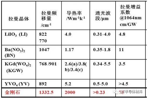
Diamond Raman Laser Research:Stimulated Raman scattering is an important nonlinear optical effect. Stimulated Raman scattering can achieve a fixed frequency displacement of all incident photons without the need for phase matching. It is an important technology for expanding the use band range of lasers. Research in this direction has become a hot spot in the development of laser technology.
Als kristallines Raman-Material mit hervorragenden Eigenschaften weist Diamant die größte Raman-Frequenzverschiebung von 1332.3 cm unter den bekannten kristallinen Materialien auf.-1, its Raman gain linewidth is about 1.5 cm at room temperature-1. The Raman gain of diamond has polarization selectivity. When the polarization direction of the pump light is parallel to the <111> direction of the diamond crystal, its Raman gain is maximum (10 cm/GW@1 μm), and linearly polarized Raman light is output. Diamond has ultra-high thermal conductivity, and its ultra-fast heat dissipation ability is the key for diamond crystals to maintain high Raman gain and obtain high-beam quality laser output under high-power operation.
Comparison between common laser Raman crystals and diamond
In recent years, with the improvement of chemical vapor deposition preparation technology, the optical quality of artificial diamond has been rapidly improved. Optical-grade diamond crystals have also shown excellent power improvement, coherence enhancement and frequency conversion capabilities with their excellent Raman and Brillouin characteristics. This has promoted diamond lasers to greatly overcome the thermal effects of particle number inversion lasers based on traditional working materials, as well as the difficulty of balancing wavelength and output power.
Wärmeableitungssubstrat für 3D-Verpackungen aus Einkristalldiamant:
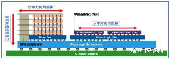
When following Moore's Law has become an industry consensus, the proposal of More Moore seems to have added some brightness to the development of the chip manufacturing industry. Generally speaking, More Moore refers to the continuous shrinking of chip feature sizes, which includes two aspects: continuing to shrink the feature size in the horizontal and vertical directions of the wafer in order to improve density, performance and reliability; using process technologies such as 3D structures and the use of new materials to affect the electrical performance of the wafer.
(Picture from Carbontech 2020 report PPT by Jiangnan researcher at Ningbo Institute of Materials)
Elektronische Gehäusematerialien dienen der Aufnahme elektronischer Bauteile und ihrer Verbindungen. Sie fungieren hauptsächlich als mechanische Stütze, Dichtung, Schutz, Wärmeableitung und Abschirmung. Sie haben einen entscheidenden Einfluss auf die Leistung und Zuverlässigkeit integrierter Schaltungen. Mit der Weiterentwicklung der Elektroniktechnologie schreiten integrierte Schaltungen in Richtung ultragroßer Dimensionen, ultrahoher Geschwindigkeiten, hoher Dichte, hoher Leistung, hoher Präzision und Multifunktionalität voran, was immer höhere Anforderungen an die Gehäusematerialien stellt. Die Forschung und Entwicklung von Hochleistungs-Gehäusematerialien für verschiedene Systeme, wie beispielsweise Diamant/Kupfer, Diamant/Aluminium, Diamant/Siliziumkarbid und Graphit/Kupfer, ist von großer Bedeutung für die Weiterentwicklung elektronischer Gehäusematerialien hin zu Miniaturisierung, hoher Leistung, hoher Zuverlässigkeit und niedrigen Kosten.
。。。。。
●Ultra-precision machining
Diamond materials and laser processing technology:Diamant zeichnet sich im Vergleich zu anderen Materialien durch einen hohen spezifischen Widerstand, eine hohe Durchschlagsfestigkeit, eine niedrige Dielektrizitätskonstante und eine geringe Wärmeausdehnung aus. Seine Anwendung im Wärmemanagement erfüllt die Anforderungen der rasant wachsenden Elektronikindustrie an hochdichte und hochintegrierte Baugruppen. Die Laserbearbeitung ermöglicht die Herstellung hochwertiger Diamantmikrostrukturen. Es handelt sich um eine fortschrittliche Fertigungstechnologie, die derzeit im In- und Ausland erforscht wird.
Diamantsubstrat-Schleif- und Poliertechnologie
Semiconductor devices mainly include integrated circuits, power devices, optoelectronic devices and sensors, etc. Power devices are widely used in aerospace, military and national defense, power energy, rail transportation, and information Internet of Things. The semiconductor wafer is the carrier of the semiconductor device, and the semiconductor substrate is the carrier of the semiconductor wafer. The substrate is the epitaxial base of semiconductor devices, which directly determines the quality and performance of the device.
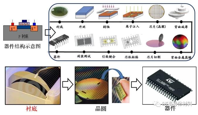
Ultrapräzise Bearbeitung
The objects of ultra-precision machining are generally small-sized diamond materials, which are too costly for industrialization and are not conducive to industrial application. To successfully apply diamond to the heat dissipation of power devices and achieve industrialization, the acquisition of large-size wafer-level heat dissipation base materials with good surface quality is a key. In addition, as the level of circuit integration on diamond substrates increases, the requirements for surface quality will gradually increase. Surface roughness will develop to the angstrom level or even smaller, and surface warpage will reach 5 μm or smaller.
Haftungsausschluss: Dieser Artikel wurde aus „DT Semiconductor Materials“ übernommen, das den Schutz geistigen Eigentums unterstützt. Bitte geben Sie die Originalquelle und den Autor des Nachdrucks an. Sollten Urheberrechte verletzt worden sein, kontaktieren Sie uns bitte, damit wir den entsprechenden Artikel entfernen können.
Verwandte Empfehlungen
Exklusivinterview mit Li Gang von Yunfan Ruida: Die Präzision von Millimeterwellen-Radarprodukten und die Wärme der Menschlichkeit
2026-07-22
2517
RF Passion, Craftsman's Journey: Over 30 Years of Steady Deadward Dedication — Interview with Kinghelm Chief Engineer Mr. Qin hongxiang
2026-06-26
2687





 粤公网安备44030002007346号