
























サービスホットライン
ニュース

ニュース
世界の半導体ソフトウェア業界は3社が支配している。
2022-03-17
851
"Shishuoxinyu" has been with you for 873 days
2019年以降の過去2年間、ファーウェイ・ハイシリコンやSMICなどの事件が相次ぎ、チップを核とする半導体技術は研究所から街へと進出し、一時期は全国的な話題となった。半導体分野で大きな影響力を持つ光発基金の劉格松氏も、公の場で資金調達を行うようになった。
同時に、海外のテクノロジー大手企業の名前がますます注目を集め、食後の話題に欠かせないものとなっている。例えば、フォトリソグラフィー装置を独占するオランダのASML、OEMメーカーとして発言権を持つ中国の台湾積体電路製造(TSMC)、そしてAndroidスマートフォンのセールスポイントとなっているアメリカのクアルコムなどが挙げられる。
But there is a segmented software productEDA (電子設計自動化), little is known about it. But in fact, EDA is as important to global semiconductors as TSMC, which is a foundry, and ASML, which is a lithography machine. It is not an exaggeration to call it the software vitality of semiconductors.
これまでのところ、この半導体ソフトウェア産業で利益を上げている中核企業は、アメリカ発祥の3社である。Synopsys, Cadence, Mentor Graphics, they have dominated the ups and downs of the global semiconductor industry with a stable gross profit margin of close to 80% in the past 30 years.
01
The ultimate division of labor creates EDA
The global market size of EDA is only about US$10 billion, but to truly understand this industry, we must put it in the context of the entire semiconductor market (the market size is close to US$500 billion), starting from the entire industry chain.
In order to turn sand (silicon) into magic and finally make almost omnipotent integrated circuits (chips), engineers need to use the most cutting-edge technology in every aspect of semiconductor manufacturing. Precisely because every field needs to push technology to the extreme, the semiconductor industry has formed an extremely special business model——The ultimate division of labor.
Looking from upstream to downstream, the semiconductor industry chain can be divided into asset-light IC design (also called fabless factory), asset-heavy manufacturing, packaging and testing. Among them, chip design companies are typically characterized by light assets and high technology. Representative companies include Qualcomm (NASDAQ: QCOM), NVIDIA (NASDAQ: NVDA), etc. They only need to hand over the designed chip layout to the middle and lower reaches of the industry chain for manufacturing and packaging testing. In order to better support these chip design companies in completing chip design work, supporting professional software and intellectual property packages, namely EDA and IP, have gradually evolved. This part is now also completed by specialized manufacturers.
IP has been explained in the article about ARM before. The focus of this article is on EDA, and IP is just brought.
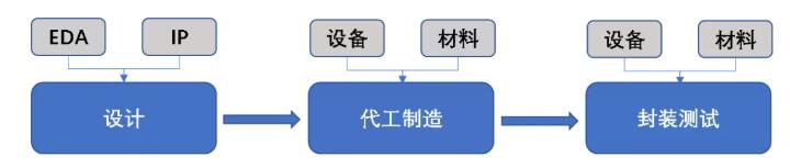
図1:半導体産業チェーン、データソース:ブロケード研究所作成
For the semiconductor industry, the essence of extreme division of labor is a risk-sharing mechanism. After all, no company can overcome all technical difficulties in the semiconductor industry, and the industry chain spares no effort to refine the division of labor, allowing each participant to push technology to the extreme in their own field.
Taking a detailed look at the history of the development of the semiconductor industry, there are three business model innovations that profoundly reflect the ultimate division of labor in the semiconductor industry and have a profound impact on the development of the industry:
【1】製造工程が分離されており、画期的な意義があります。
製造工程の分離によって半導体製造の敷居が大幅に下がり、資金力のない草の根チームでも反撃が可能になった。ファウンドリ製造に特化したTSMCを例にとってみよう。最先端の精密製造技術を習得することで、ムーアの法則を強力に推進する存在となった。
Precisely because TSMC has solved manufacturing problems, startups do not necessarily need to choose the asset-heavy IDM (Integrated Device Manufacture) model. Most of them turn to fabless, that is, fabless design companies. After gathering a few smart design engineers, they can roll up their sleeves and start working.
この分野で最も代表的な企業は有名なTSMCであり、A株市場に上場しているのはSMICです。この分野については皆さんもよくご存知でしょうから、ここでは詳しく説明しません。
Figure 2: TSMC
【2】The birth of professional software liberated IC design engineers
しかし現実には、TSMCだけでは十分ではありません。チップを設計する際には、数億個ものトランジスタと関連回路を1平方センチメートルあたりの狭いスペースに配置する必要があるからです。これは明らかに人間の手作業の能力をはるかに超えています。自動設計を実現するために、EDAソフトウェアが誕生しました。
EDA, the full name of Electronic Design Automation, is electronic design automation. When engineers design chips, they only need to use programs to plan chip functions, and then use EDA tools to convert the programs into actual circuit design drawings. Therefore, EDA is essentially a special industrial software, but it is famous for its application in the chip field and has become an essential toolbox for every chip design engineer.
この分野における独占企業は、誰もが知っているわけではありません。代表的な企業としては、Synopsys、Cadence、Mentorなどが挙げられます。国内ではまだ上場している企業はありませんが、BGI Jiutian、Guangliweiなどが証券会社から指導を受けており、将来的にIPOが実現するでしょう。

Figure 3: Synopsys
【3】産業の発展に伴い、知的財産の概念が徐々に生まれてきた。
The innovation of design automation is not limited to the birth of EDA. During the process of designing chips, engineers found that many things can be reused, that is, "modular". Therefore, some companies that only do this part specialize in designing IP cores (Intellectual Property Core).
IPコアとは、独立した知的財産権を持つ設計マクロモジュールであり、チップ設計において再利用可能です。これらの成熟した信頼性の高いIPソリューションは特定の機能を実現できるため、チップ設計企業は設計用にIPコアを購入することができ、チップ設計プロセスを大幅に簡素化できます。進化を経て、IPコアはシステム設計における基本単位となりました。
この分野で最も有名な企業はARMであり、前回の記事「ARM:中国チームに残された時間は少ない」で詳しく解説しました。特に注目すべきは、トップクラスのIP企業の多くがEDA企業であることです。実際、これは理解しやすいことです。なぜなら、日々自動設計ソフトウェアを開発している企業は、IPコアについて既に熟知しているからです。現在、A株上場企業の中には、IPコアを主力事業とする企業も存在します。VeriSilicon(SH:688521)。
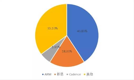
図4:世界の半導体IP市場の概況(2019年)、出典:IPnest
上記3つの重要なビジネスモデル革新こそが、半導体産業が従来産業とは全く異なるビジネスモデルを形成した理由である。設計プロセス全体の簡略図を以下に示す。C言語設計会社、ファウンドリ企業、EDAソフトウェア企業、IPプロバイダーが緊密に連携し、非常に強固な「鉄の三角形」関係を築き、共同で迅速な製品開発と反復開発を完了させ、チップのコストを大幅に削減している。
EDA、IP、ファウンドリのおかげで、この業界における起業のハードルは大幅に下がり、多くの国内企業が10年余りで急速に成長できることが証明されました。Weill Technology、Shengbang Technology、GigaDevice、Hengxuan Technology、Star Semiconductorなど、これまで多くの企業がこのモデルを採用してきました。
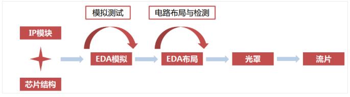
Figure 5: Product production process of Fabless mode chip design companies, source: Semiconductor Industry Observation, Founder Securities
02
I am very young, but I am the lifeblood of semiconductors
【1】I am small, but I am crucial
100億ドル近くにも及ぶファウンドリ市場とは異なり、半導体分野におけるEDAとIPは、極めて細分化された分野である。これらはチップ産業チェーンの最上位に位置するため、市場規模は実際には非常に小さい。数十年にわたる発展を経て、世界のEDA市場は数百億ドルの規模に達する見込みだが、IP市場はさらに小さく、世界市場シェアの40%近くを占める大手ARMの売上高でさえ、2億ドル未満に過ぎない。
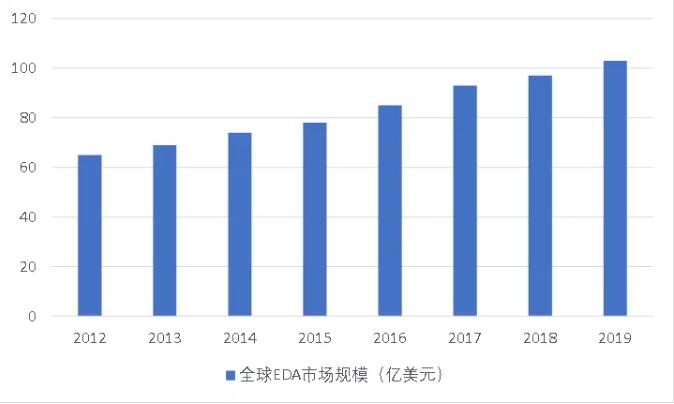
図6:世界のEDA市場規模は約10億米ドルに過ぎない。出典:EDAC
規模は小さいとはいえ、EDAとIPがなければ世界の技術発展は停滞すると言っても過言ではない。
存在するシノプシスOn the official website of , there is a picture that depicts this relationship very accurately:Although the total market size of EDA and IP is only more than 10 billion US dollars, the entire electronic system of 1.65 trillion US dollars is based on this, forming a typical inverted pyramid model.. In other words, without EDA and IP, the entire pyramid will collapse.
さらに、EDAとIPの開発は非常に困難です。チッププロセスの微細化やプロセスパラメータの変更などに伴い、絶え間ない反復作業が必要となり、各反復作業ごとに基盤となるコードの更新が大量に発生します。今日では、人工知能とIoTの時代が到来し、ポストムーア時代の制約下において、この分野のイノベーションはより大きな課題に直面しています。
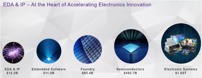
Figure 7: EDA and IP are the core of semiconductor innovation, source: Synopsys official website
[2] EDA&IPの観点から見た中国と米国の基礎研究の格差の検証
この業界における技術的な障壁が時間とともにますます高くなっているのはまさにそのためであり、現在、EDA分野に残っている巨大企業は、Synopsys、Cadence、Mentor Graphicsの3社のみである。, these three "old companies" with a history of more than 30 years can be said to be the originators of EDA:
-
概要:1986年に設立されたアメリカの企業で、アールト・デ・ゲウス率いるゼネラル・エレクトリックのエンジニアチームによって設立されました。2008年には世界トップのEDAソフトウェアツール企業となり、近年は年間売上高が3億米ドルを超え、現在もその地位を維持しています。
-
ケイデンス:1988年設立のアメリカ企業。1992年には既にEDA業界のリーダー企業となっていたが、2008年にシノプシスに追い抜かれた。シノプシスの現在の売上高は2億ドルを超えている。
-
メンター:1981年設立の、アメリカで最も歴史のある企業です。EDAツールの包括性はシノプシスやケイデンスに劣るため、売上高は約1億ドルですが、PCB設計ツールなど一部の分野では比較的先行しています。メンターは2016年にドイツのシーメンスに買収されました。
上記の3大企業はいずれもアメリカ発祥の企業で、市場シェアの合計は70%を超えています。まさにこの時、ファーウェイは封鎖に直面しました。業界は、EDAソフトウェアの販売が制限されれば、中国のチップ設計業界は大きな打撃を受けるのではないかと懸念していました。そして、私たちには、これについてできることは何もないと言えるでしょう。
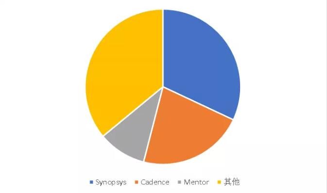
図8:EDAソフトウェアのグローバル競争環境、出典:千站工業研究所
Naturally, some people will ask, since it is software, if it is restricted, can I make each cracked version first? The answer is no. As mentioned earlier, EDA software does not remain unchanged after being written. With changes in downstream applications, changes in materials, and improvements in manufacturing processes, EDA needs to constantly iterate to update the process library, most frequently once a month. To give an analogy that may not be appropriate, if your office requires major upgrades every month before it can be used, then there will naturally be no room for pirated versions to survive.
このソフトウェアは基本的にクラック不可能であることに加え、ユーザーの定着率が非常に高い。一方で、EDAソフトウェアはこれらの企業のコスト項目のごく一部を占めるに過ぎず、価格変動に全く敏感ではない。非常に重要なソフトウェアであるため、顧客はやむを得ない事情がない限り、サプライヤーを変更することはまずない。他方、EDAの本質は、顧客に問題解決のためのツールキット一式を提供することにある。これらの海外大手企業は、ワンストップサービスを提供できるのだ。
したがって、シノプシスをはじめとする企業は、強力な競争優位性を持つ知的財産権に依拠することで、半導体産業の発展による恩恵を享受することができる。
At present, Chinese EDA companies are still in their infancy. Well-known companies include BGI9, Guangli Micro, and Boda Micro. However, their manufacturing processes are above 20nm and they cannot provide a full set of tools. As a result, they are quite passive in the competition and face many challenges. But behind the challenges are greater opportunities. With the rise of independent brands in the domestic semiconductor industry and the emphasis on intellectual property rights, domestic EDA companies finally see the opportunity to turn around.
03
別の山からの石:Synopsysをリファレンスとして使用する
Know yourself and your enemy, and you can fight a hundred battles without danger.
EDA分野の絶対的リーダーであるシノプシスは、13年間トップの座を維持してきました。さらに、近年の業界動向に対応してIP事業を急速に発展させ、現在ではIP分野でARMに次ぐ世界第2位にランクされています。EDAとIPは半導体の生命線とも言えるものであり、シノプシスは生命線の門番と言っても過言ではありません。ブロケード・リサーチ・インスティテュートは、EDA&IP分野のリーディングカンパニーであるシノプシスを、財務的な観点から分析します。
【1】金融データは偽物と同じくらい安定している
1991年に入手可能な同社の最も古い財務データによると、分析後の最初の印象は安定しているということである。ここでは、同社の売上高と粗利益率という2つの指標を選択する。
1) Revenue has grown steadily from US$40 million to US$3.7 billion, with an average annual growth rate of 17%. You can hardly see the shadow of cycles in it. There has been no year of revenue decline after 2005;
2)粗利益率はさらに誇張されている。過去30年間、会社の売上高や事業構造の変化に関わらず、約80%で安定しており、これは偽りの数字のように見える。
同社の最新の半期決算報告によると、2021会計年度上半期の売上高は2億米ドルで、前年同期比17.6%増、粗利益率は79%で、過去30年間の安定した業績と再び一致している。驚きを禁じ得ない。「兄弟よ、安定している」。
It is under the steady growth that the company's market value has grown from the initial US$400 million to the current US$38 billion, becoming an out-and-out "bull stock".
Another leading company, Cadence(チェンテン・エレクトロニクス)また、同様の特徴も示しています。このような驚異的な財務指標が存在する理由は、この業界の技術的な障壁が非常に高く、顧客の定着率が極めて高く、価格変動に鈍感であるためです。これらの企業は、干ばつや洪水といった不況下でも収益を維持し、休眠状態でも安定した利益を上げることができるのです。
But it is precisely for this reason that you hardly need to expect these companies to have disruptive innovations, nor do you need to expect explosive growth in a certain year. They are basically a green train with high safety, moving forward at a leisurely pace. Of course, this has also become one of the key points of criticism for the company. After all, most of the people who study this field are growth stock hunters.
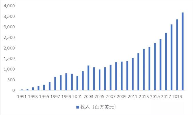
図9:シノプシス社の売上高、データソース:ブルームバーグ
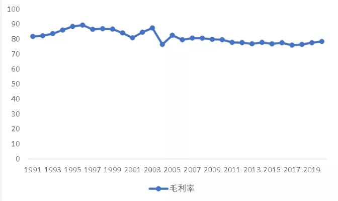
Figure 10: Synopsys gross profit margin, data source: Bloomberg
【2】Secrets to establishing competitive advantages in the EDA industry:エンジニアの異常な集団と、テクノロジーの異常な購入
前述の通り、同社の成長率と粗利益率は驚くほど安定しており、これは基本的にテクノロジー業界において異例の存在と言えるでしょう。私たちがよく知るテクノロジー業界は、「トップ・オブ・ザ・ウェーブ」に登場するような企業群に近いものです。各社が数年間トレンドを牽引し、浮き沈みを繰り返してきました。しかし、EDA分野のこれらのグリーンカーは30年以上も安定して事業を継続しており、今もなお健在です。この結果から、この業界が強固な競争優位性を持っていることは容易に推測できます。そうでなければ、粗利益率の80%は新規参入企業によって押し下げられていたはずです。
シノプシスに戻ると、その最大の強みはその包括性にある。アナログフロントエンドにはXA、デジタルフロントエンドにはVCS、バックエンドにはサインオフツールなどを備えており、そのツールの中には非常に強力なものもある。TCADデバイスシミュレーション(注:EDAソフトウェアの中核となる最下層)の90%、DFMプロセスシミュレーションの50%を独占している。下流の顧客が複数のサプライヤーをサポートする必要がなければ、理論的にはシノプシスの市場シェアはさらに高くなるだろう。
シノプシスの競争優位性を支える秘訣は一つThe business model of crazy engineers高度な知能を必要とする人材を大量に集める結果、研究開発費が高額になる。
前述の通り、EDA分野では絶え間ないアップデートと反復開発が求められるため、極めて巨額の研究開発投資が必要となります。シノプシスの年間収益の3分の1は研究開発に投資される必要があり、2020年までに年間研究開発投資額は1.3億米ドル近くに達する見込みです。今後、業界の技術的課題が増加するにつれ、人件費もますます高騰していくでしょう。1.3億米ドルは、まさに新たな段階の出発点に過ぎません。
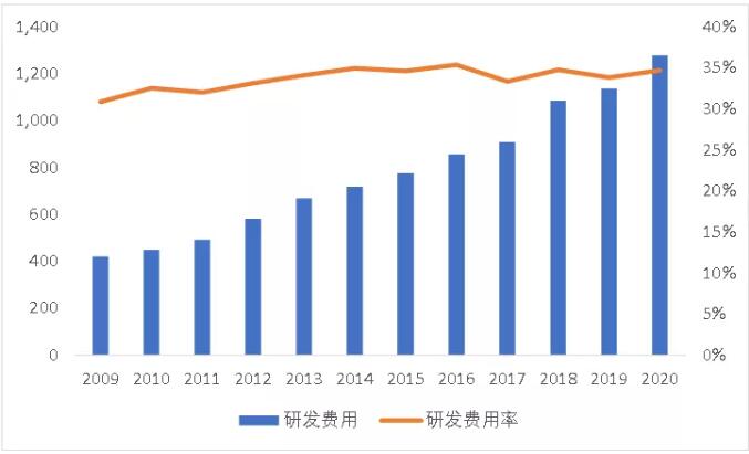
図11:シノプシスの極めて高い研究開発費、出典:ブルームバーグ
In addition to internal research and development, this industry also needs constant external mergers and acquisitions. Since its establishment in 1986, Synopsys has made 80 mergers and acquisitions., the targets of mergers and acquisitions are basically products and companies that have been proven successful by the market. Technology integration is carried out through mergers and acquisitions. Longer and Longsan Cadence (Chenteng Electronics) and Mentor Graphics (Mentor International) have also conducted more than 60 mergers and acquisitions respectively.
On the surface, mergers and acquisitions appear to be the acquisition of other companies and an investment behavior, but in fact they are the externalization of R&D expenses as an effective supplement to internal R&D.
It is precisely by relying on high-level internal R&D and continuous external mergers and acquisitions that Synopsys has achieved a business model that is easy to defend but difficult to attack, enabling it to achieve stable growth and make money on its own.
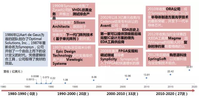
図12:シノプシスによる重要な買収案件(出典:ファウンダー・セキュリティーズ)
【3】The Chinese market will become the new main battlefield for EDA
In the past, the Chinese market was an insignificant existence, but in recent years, with the emergence of domestic chip design companies, revenue from China has become an important source of Synaptics.In fiscal year 2020, China’s revenue accounted for 11.4% of the company’s revenue(注:この比率は中国製チップの自律性率にも似ています)米国に次ぐ第2位の市場となります。
In the future, with the rise of China's chip design industry, as the gatekeeper of semiconductor software, Xinsi's revenue share in China will continue to increase, and China will become an important source of its growth. Of course, domestic EDA companies are obviously also eyeing this big opportunity. As they gradually go public, they may make bigger moves. We still need to wait for their disclosure of prospectuses before we can have more interpretations.
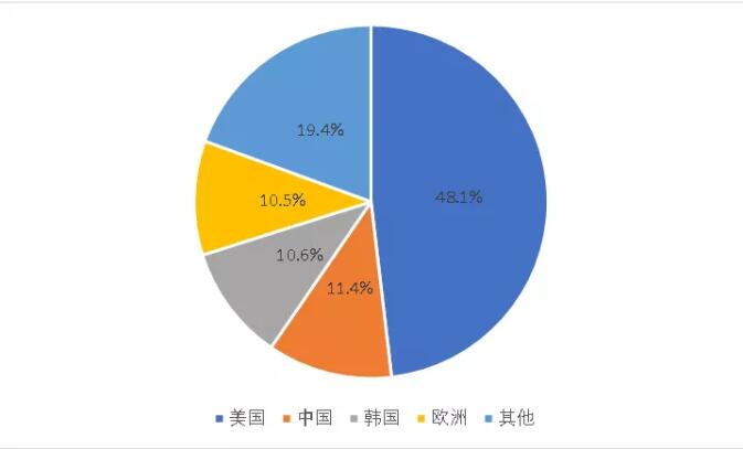
Figure 13: Synopsys revenue broken down by geography (fiscal year 2020), Source: Synopsys
しかし、注目すべき点が一つある。ローカライゼーション意識の急速な高まりと、国内エンジニアへの配当金の波が押し寄せる中で、シノプシスが世界中で収益を上げてきたビジネスモデルを中国にそのまま適用できるかどうかは、確かに大きな疑問符となる。
After all, there is an old saying in China,How can I allow others to sleep soundly on the couch?。
Disclaimer: This article is reproduced from "Shishuoxinyu". This article only represents the author's personal views and does not represent the views of Sacco Micro and the industry. It is only for reprinting and sharing and supports the protection of intellectual property rights. Please indicate the original source and author for reprinting. If there is any infringement, please contact us to delete it.
会社の電話番号:+86-0755-83044319
ファックス番号:+86-0755-83975897
Eメール:1615456225@qq.com
QQ: 3518641314 李マネージャー
QQ: 332496225 邱マネージャー
住所:深圳市龍華新区民治大道1079号 占濤科技ビルC棟809室
関連する推奨事項
雲帆瑞達の李剛氏独占インタビュー:ミリ波レーダー製品の精度と人間性の温かさ
2026-07-22
2534
また来年! | Slkor at 2026 electronica China ハイライトまとめ
2026-07-14
2220
RFへの情熱、職人の歩み:30年以上にわたる揺るぎない献身 ― キングヘルム社チーフエンジニア、秦宏祥氏へのインタビュー
2026-06-26
2696
数万もの企業が中国ブランドを選択 ― KinghelmとSlkorは世界中で好調な売れ行きを見せている!
2026-06-24
2442
2連覇後もなお、我々は前進し続けている――スン・ガオフェイへのSlkorインタビュー
2026-06-11
2463





 粤公网安备44030002007346号