
























Service Hotline
News

News
Analysis of technical characteristics and development trends of high-power IGBT drives
2022-03-16
1344
1 Introduction
becauseigbthaveswitchDue to its high frequency, low conduction power consumption and convenient gate control, it has been widely used in high-power conversion systems. In igbt applications, in addition to its own technical level, another important factor to consider is whether the design of its driver is reasonable and reliable. igbt drive as powercircuitbetween the controller and theinterfaceThe circuit is closely related to the power consumption and reliability of the system. An optimized driver is indispensable in the power conversion system. Choosing an appropriate driver circuit is closely related to the reliability of the overall converter solution.
The driver mainly completes the following three functions. The first is the driving function, which provides a large enough drive for the igbt switch.current, to ensure that igbt can be reliably turned on and off under its control; secondly, the driver must have a protection function. When igbt occursshort circuitOr when there is overcurrent, the driver can turn off the igbt in the shortest time to protect the power device.In addition, in high-voltage and high-power applications, the driver, as a connecting bridge between the control circuit and the power circuit, must have the function of electrical isolation to ensure that the control circuit will not be interfered with and affected by the power circuit.On the premise of satisfying the above three functions, the driver must also consider the relationship between flexibility, performance and price.
Due to the different current capacities and voltage levels of IGBT, there are also differences in the technical requirements for its drivers. In low-power applications, because the driving current is relatively small, integrated drivers are mostly used. In high-power and high-voltage applications, such as high-power UPS power supplies, high-voltageFrequency converteretc., requiring the driver to provide larger drive current, higher isolation voltage and more complete protection functions. This article focuses on the commonly used high-power IGBT drive modules currently on the market, such as Semikron's SKHI22 and Concept's 2SD315A, etc., and analyzes some of their common technical features, design points, and future development trends of high-power IGBT drive technology.
2 Analysis of technical characteristics
2.1 Complete signal processing functions
In high-voltage and high-power applications, it is very important to ensure the reliability of the IGBT drive signal, considering factors such as the strong interference generated by the switch and the high cost of IGBT. Therefore, high-power igbt drive modules usually have a complete drive pulse signal preprocessing function, whose purpose is to ensure the reliability of the pulse signal of the igbt gate. Common drive signal processing functions are as follows:
(1) Dual-channel pulse interlocking function
When the drive module outputs two pulse signals to control the upper and lower IGBTs on the same bridge arm respectively, if the drive signal controls the conduction of two IGBTs at the same time, a through short circuit will occur, which may cause damage to the IGBT or other devices. In order to prevent the above situation, a signal interlock circuit is designed inside the driver module to ensure that when the two input pulse signals are high at the same time, the two outputs are low at the same time to prevent shoot-through. When independent control of dual drive signals is required, the interlocking function can also be shielded through external terminals.
(2) Narrow pulse suppression function
The narrow pulse signal caused by the control circuit or interference, etc., is added to the gate of the IGBT through the driver, which may cause the IGBT to complete a switching process in a short time. A too short pulse signal causes the IGBT to turn off before it is fully turned on, which has a negative impact on the output of the converter, increases the switching loss of the IGBT, and reduces the efficiency of the system. A filter circuit is designed in the driver to remove narrow pulse signals, which is beneficial to improving the reliability of igbt.
(3) Dead time setting function
In the half-bridge working mode, the two IGBTs must be turned on in turn. In order to prevent the two IGBTs from being turned on at the same time during the switching process, a certain dead time must be added when the two tubes are alternately turned on. According to the IGBTs with different characteristics, the dead time is different. In the dual-channel high-power drive module, a dead zone control circuit is designed internally, and the size of the dead zone can be adjusted through different connection methods of external terminals, such as by connecting external terminals of different capacities.capacitance(2sd106) or high and low level (skhi22a/b).
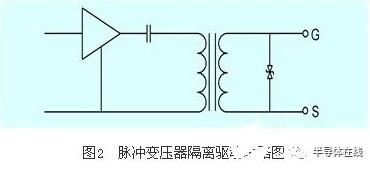
Figure 1 shows semikromThe signal processing block diagram of the company's igbt high-power driver [3] includes various signal processing functional modules, whose purpose is to ensure the reliability of the igbt drive signal.
2.2 Isolated transmission method of driving signals
Considering that the high-voltage and high-power IGBT driver works in a high-voltage environment, in order to ensure that the controller is not affected by the high-voltage side, the drive pulse signal must be isolated and then transmitted to the gate of the IGBT. Common isolation methods include optical isolation and magnetic isolation. Optical isolation includesOptocouplerisolation andoptical fiberIsolation, optocoupler isolation method has problems such as transmission delay, aging and reliability due to the relatively low isolation voltage. It is rarely used in high-voltage applications where the DC bus voltage exceeds 800v. And adoptpulse transformerIsolation method (magnetic isolation) can achieve relatively high isolation voltage, andtransformerIt has high reliability, small transmission delay, can achieve higher switching frequency, and does not have aging problems. Therefore, most of the high-voltage igbt drivers use pulse transformers as isolation components to complete the isolation transmission of drive signals.
The traditional driving pulse transformer isolates the amplified pulse signal and directly drives the IGBT or power MOS tube. Its basic circuit principle is shown in Figure 2. The function of the primary series capacitor is to remove the DC component of the drive pulse. The secondary parallel voltage regulator tube is used to prevent the output voltage from being too high and damaging the power switch tube. This working method does not require a separate driving power supply, the circuit design is simple, and the cost is relatively low. However, when the duty cycle of the driving pulse varies widely, especially when the duty cycle is relatively large, since the volt-second area of the transformer output waveform in one cycle must be equal, the amplitude of the output positive pulse may be reduced, making it impossible to drive the igbt normally. The control pulse duty cycle is usually required to be less than 50%. At the same time, the pulse transformermagnetic coreThe saturation problem also limits the on-time of the control pulse. Another disadvantage is the distortion of the driving waveform, especially when driving high-power IGBT. Due to the relatively large input capacitance of IGBT, the driving pulse waveform of the secondary output of the pulse transformer is difficult to meet the driving requirements. Therefore, this driving method is mainly used in low-powerswitching power supplymiddle.
For high-voltage and high-power IGBT, the above driving method obviously cannot be applied. The commonly used method is to modulate the driving pulse signal and convert its rising edge and falling edge into two inverted narrow pulse signals. The pulse transformer just converts these two pulse signals.couplingto the secondary level, and then restore the driving pulse signal through the secondary reconstruction method. Its working principle is shown in Figure 3.
This method can be called pulse edge coupling transmission method. The advantage of this method is that the pulse transformer only transmits narrow pulse signals with a fixed pulse width and can adapt to driving pulse signals with a wide range of duty cycle changes. Since the transformer transmits narrow pulse signals, the core and windings of the transformer can take relatively small values, and the corresponding leakage inductance and distributed capacitance are also relatively small, which is beneficial to the design of the pulse transformer and signal transmission. The disadvantage is that the conversion and reconstruction circuit is added, and the circuit is relatively complicated. Figure 4 shows the primary experimental waveform of the pulse transformer after conversion.
In order to facilitate users to design the drive power supply, high-power igbt drive modules usually come with a dc/dc converter inside. DC/DC converters with high isolation voltage levels do not require users to separately design an isolated power supply. Integrated isolation converters usually adopt a half-bridge or push-pull structure. In order to increase the isolation voltage and simplify the converter control circuit, they generally do not have closed-loop control. Some drivers add a linear regulated power supply at the output end to stabilize the driving voltage. In order to reduce the size of the transformer, the operating frequency is mostly above 100khz. In high-voltage and high-power applications, depending on the bus voltage, the driver must have a high isolation voltage tolerance between the primary and secondary. A bus voltage of 900vdc requires at least an isolation voltage of 4kv ac. Another factor that must be considered is the dv/dt tolerance. When the igbt switches at high speed, a very high dv/dt may be generated. This signal can be coupled to the primary control circuit through an isolation transformer or pulse transformer, causing interference to the control circuit. Therefore, when designing the isolation transformer, it is also required to have a very small primary and secondary coupling capacitance. The size of the transformer coupling capacitance is determined according to the specific requirements for dv/dt endurance, which is usually less than 20pf.
The manufacturing process of the transformer is the key to achieving the above-mentioned high isolation voltage. In order to increase the isolation voltage tolerance and reduce the coupling capacitance between the primary, secondary or secondary, the windings are usually wound separately and separated by insulating baffles. Sometimes it is necessary to coat the surface of the magnetic core with thickened insulating material or wind it with three layers of insulated wire. Figure 5 is a schematic diagram of the transformer structure of eupec's igbt driver module 2ed300c17 [4].
2.4 Short circuit protection and threshold adjustment
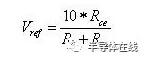
The currently commonly used igbt short circuit or overcurrent protection method is realized by detecting the voltage value of vce [5]. When the igbt has a short circuit or overcurrent, its working area will exit the saturation zone and the vce voltage will increase. Specifically,protection circuitThe principle is shown in Figure 6. passdioded is connected to the collector of igbt to realize the undersaturation detection of igbt. The increase in vce voltage will correspondingly increase the anode potential of the series diode. When the set short-circuit threshold is exceeded, the protection circuit will act and shut down igbt. Since the collector voltage of IGBT is relatively high in the early stage of turn-on, if the protection circuit operates at this time, it may cause malfunction. A dead zone time must be set, during which the short-circuit protection circuit will not work. This function is connected in parallel via switch s and an externalresistanceIt is realized by rce and capacitor cce. When igbt is turned off, s is turned on, and capacitor cce is charged to 15v. When igbt is turned on, s is turned off, and the cce capacitor is discharged through rce. The discharge end voltage is:
This can make the reference voltage higher than the detection voltage in the early stage of igbt turn-on, preventing the protection circuit from malfunctioning. The waveform during normal operation is shown in Figure 7(a). The waveform when a short circuit or overcurrent fault occurs is shown in Figure 7(b).
2.5 User interface method
In order to adapt to igbt modules packaged by different manufacturers, the igbt driver must have a user-friendly interface. It also requires extensive flexibility and economical cost. Common driver modules currently on the market mainly useweldingImplement the connection with igbt on the pcb board, such as: skhi22, 2sd315a and 2ed300c17, etc. In order to facilitate installation, a direct plug-in connection method is also used. Figure 8 is the appearance of the skyper driver module developed by semikron. It is connected to the drive interface board in a plug-in manner.
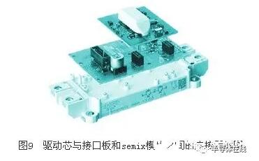
Since the drive module (drive core) only provides the most important common functions in the drive, its connection with different modules in different applications needs to rely on the interface board. The entire module-drive unit includes a power module with a spring interface, a standard or enhanced drive core, and an interface board that connects the drive core to the specified module. The interface board that can be customized has an outstanding advantage: the user can adjust and determine the switching characteristics of the igbt by himself, for example: changing the speed of igbt opening or closing by adjusting rgon or rgoff; adjusting the dead time or disabling the interlock function; adjusting the vce protection point and window time, etc. Compared with the intelligent power module ipm currently on the market, the interface board makes the entire system more flexible and easier to adapt to different applications. Once the system parameters are set, the entire system can be used as easily as ipm. The electrical connection between the semix module and the interface board is through the spring built in the semix module and the bottom layer of the interface board.Contactto achieve. After assembly, the contacts of the interface board touch the spring contacts of the module, completing the electrical connection through pressure contact. Contact pressure increases the reliability of the power module compared to soldering technology. Similarly, the plug-in connection between the drive core and the interface board is also to avoid welding [6]. Figure 9 is an example diagram of the connection between the driver core, interface board and semix module.
2.6 Highly integrated
The development trend of the driver is to be highly integrated, which can reduce the size of the driver and be more closely integrated with the igbt, making it easier to install, reducing the length of the connection lines between the driver igbt modules, and reducing the leadsinductance. In order to achieve this goal, the igbt driver modules currently developed by some foreign companies all use self-developed specialintegrated circuitasicFor example: Semikron's skic2001a and Concept's ldi001 and lgd001. Through the application of ASIC, most of the control and protection functions can be implemented with IC, which greatly reduces the size of the drive and increases the reliability of the igbt drive.
3 Development trends of high-voltage and high-power igbt drive modules
As a composite power semiconductor, igbt is being used more and more widely, especially in high-power converters, due to its low power consumption, high switching frequency and large current capacity. The requirements for its drive circuit will also become higher and higher. The main technical development directions are reflected in the following aspects.
(1) Higher integration
At present, the size of high-power igbt driver modules is still relatively large. In order to increase the isolation voltage withstand, a transformer is usually used to achieve isolation. The size and weight of the transformer are relatively large, and it is difficult to integrate. Therefore, future drives will use smaller, easier to integrateIsolatorcomponents, such as applying piezoelectric transformers or advanced magnetic integration technology to reduce the size and weight of isolation components and increase integration [7]. It is foreseeable that in the future, high-power IGBT and its drive circuit will be integrated into the same module. Users only need to directly introduce the control signal into the power module to control the IGBT.
(2) Higher isolation voltage
Current drivers use optocouplers and transformers to achieve isolation. The advantage of optocouplers is their small size, but they have shortcomings such as relatively low isolation voltage, easy aging, and large delay. Transformer isolation has a higher isolation voltage and smaller delay, but is larger. Therefore, when high-voltage isolation is required, transformers are mostly used to achieve isolation. Currently, the highest isolation voltage of a transformer-isolated drive module is about 3300v. The highest voltage level of igbt has reached 6500v. In order to adapt to higher voltage applications, drivers with higher isolation voltage must be used.
(3) Greater driving power
The capacity of igbt modules is constantly increasing, and the current capacity of a single module can already reach 3600a. Sometimes in order to increase the capacity, it is usually operated in parallel, which also puts forward higher requirements for the driving power of the driver. The maximum output current of the driver must be increased accordingly, especially when multiple modules are used in parallel, the average output power of the driver is required to reach 5w~10w, and the instantaneous maximum output current is required to reach more than 30a.
(4) Higher switching frequency
In order to adapt to applications in induction heating power supplies, the switching frequency of igbt continues to increase. With the development of manufacturing technology, the highest switching frequency of igbt can already be above 100khz, which can partially replace the power mos tube. For the driver, it means that it must provide greater drive power, and the driver must have shorter drive pulse delay time and rise and fall times, and provide greater instantaneous maximum drive current, etc.
(5) More complete functions
The currently widely used gate drive technology cannot control the di/dt and dv/dt caused by the igbt switching process, thereby controlling the emi of the conversion circuit. Active gate drive technology can effectively control the higher di/dt and dv/dt caused by igbt switching. Accordingly, it can make igbt work in a safer working area, reduce the emi generated during its switching process, and accordingly reduce the igbt buffer absorption circuit. Among them, the three-stage active gate drive technology is an active gate drive technology with wide application prospects [8]. In addition, in order to meet the needs of series and parallel IGBT applications, the driver must also have dynamic voltage and current sharing functions.
4Conclusion
As a key power semiconductor device in power electronic systems, IGBT has continued to grow for several years. As it enables power electronic devices and equipment to achieve higher efficiency, higher switching frequency and miniaturized design of power conversion devices, with the continuous improvement of performance, the application fields of IGBT devices have expanded to a wider range. Not only in industry, but also in many other power conversion systems, it has replaced high-power bipolartransistor(gtr), power mosfield effect transistor(mosfet), even an alternative gate shut-off occursThyristor(gto) realistic trends. High-power IGBT driver module technology will continue to improve, and the integration level will also increase, thereby reducing IGBT power consumption and EMI, and improving system reliability. With the development of igbt manufacturing technology and the further increase in application fields, the requirements for the performance of its drives are also constantly increasing. In order to adapt to the performance of the new generation of igbt, various drive manufacturers are developing igbt drive products with more complete performance.
Disclaimer: This article is reproduced from "Semiconductor Online". This article only represents the author's personal views and does not represent the views of Sacco Micro and the industry. It is only for reprinting and sharing to support the protection of intellectual property rights. Please indicate the original source and author for reprinting. If there is any infringement, please contact us to delete it.
Related Recommendations
Exclusive Interview with Li Gang of Yunfan Ruida: The Precision of Millimeter-Wave Radar Products and the Warmth of Humanity
2026-07-22
2542
RF Passion, Craftsman’s Journey: Over 30 Years of Steadfast Dedication — Interview with Kinghelm Chief Engineer Mr. Qin hongxiang
2026-06-26
2707





 粤公网安备44030002007346号