
























Service Hotline
News

News
Process | Ten steps to explain the chip photolithography process in detail!
2022-03-17
1204
In the manufacturing process of integrated circuits, there is an important link——Lithography, precisely because of it, we can implement functions on tiny chips. Modern engraving technology can be traced back 190 years. In 1822, after experimenting with light on various materials, the Frenchman Nicephore Niepce began to try to copy an impression (pattern) etched on oil paper. He placed the oil paper on a glass slide, and the glass slide was coated with asphalt dissolved in vegetable oil. After 2 or 3 hours of sun exposure, the asphalt in the light-transmitting part has obviously hardened, while the asphalt in the opaque part is still soft and can be washed away by a mixture of rosin and vegetable oil. By etching a glass plate with strong acid, Niepce produced a replica of Bishop d’Amboise’s engraving in 1827.
More than 100 years after Niepce's invention, during World War II, it was first used to make printed circuit boards, that is, making copper circuits on plastic boards. By 1961, photolithography was used to produce a large number of tiny transistors on Si, with a resolution of 5um at that time. Nowadays, in addition to visible light lithography, higher resolution methods such as X-ray and charged particle scribing have emerged.
The so-called photolithography, according to the definition of Wikipedia, is an important step in the semiconductor device manufacturing process. This step uses exposure and development to depict geometric structures on the photoresist layer, and then transfers the pattern on the photomask to the substrate through an etching process. The substrate mentioned here not only includes silicon wafers, but can also be other metal layers and dielectric layers, such as glass and sapphire in SOS.
photolithographicBasic principlesIt uses the characteristics of photoresist (or photoresist) to form corrosion resistance due to photochemical reaction after being exposed to light, and the pattern on the mask is etched onto the surface to be processed.
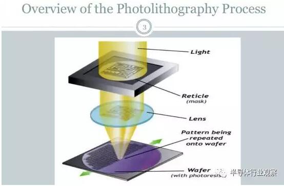
Lithography principle intention
Lithography is not a simple process, it goes through many steps:
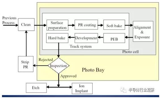
photolithography process
Let’s introduce the photolithography process in detail:
1.Wafer Clean
The purpose of cleaning silicon wafers is to remove contaminants, remove particles, reduce pinholes and other defects, and improve photoresist adhesion.
Basic steps:Chemical cleaning - rinsing - drying.
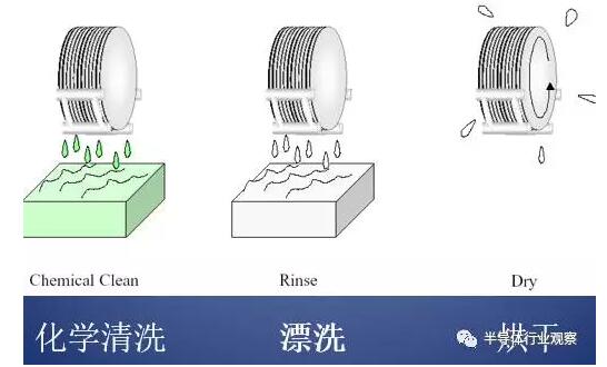
After silicon wafers have been processed through different processes, their surfaces have been severely contaminated. Generally speaking, contamination on the surface of silicon wafers can be roughly divided into three categories:
A. Contamination by organic impurities:It can be removed through the dissolution of organic reagents and ultrasonic cleaning technology.
Remove.
B. Particle contamination:Physical methods can be used to remove particles with a particle size ≥ 0.4 μm using mechanical scrubbing or ultrasonic cleaning technology, and megasonic waves can be used to remove particles ≥ 0.2 μm.
C. Metal ion contamination:Chemical methods must be used to clean the contamination. There are two major categories of metal impurity contamination on the surface of silicon wafers:
??
a. One type is that contaminating ions or atoms are dispersed and attached to the surface of the silicon wafer through adsorption.
b. The other type is that positively charged metal ions obtain electrons and then attach (such as "electroplating") to the surface of the silicon wafer.
silicon polished waferThe purpose of chemical cleaning is to remove this contamination, generally the following methods can be used to clean and remove contamination.
?
a. Use a strong oxidizing agent to cause the metal ions attached to the silicon surface to be "electroplated", oxidized into metal, dissolved in the cleaning solution or adsorbed on the silicon wafer surface.
? ?
b. Use harmless small-diameter strong positive ions (such as H+) to replace the metal ions adsorbed on the surface of the silicon wafer and dissolve them in the cleaning solution.
? ?
c. Use a large amount of deionized water for ultrasonic cleaning to eliminate metal ions in the solution.
??
Since the immersion RCA chemical cleaning process proposed by the American RCA Laboratory in 1970, it has been widely used. In 1978, the RCA Laboratory also launched the megasonic cleaning process. In recent years, various cleaning technologies based on RCA cleaning theory have been continuously developed, such as: the American FSI Company introduced centrifugal spray chemical cleaning technology, the American original CFM Company introduced the Full-Flow systems closed overflow cleaning technology, and the American VERTEQ Company introduced a chemical cleaning technology between immersion and closed type (such as Goldfinger Mach2 cleaning system), the double-sided sassafras cleaning technology of the American SSEC company (for example, M3304 DSS cleaning system), Japan's chemical-free dielectric ionized water cleaning technology (cleaning with dielectric ultrapure ionized water), which has brought the surface cleaning technology of polished wafers to a new level, and HF/O3-based silicon wafer chemical cleaning technology.
2.Pre-bake and Primer Vapor
Since photoresist contains solvent, the silicon wafer coated with photoresist needs to beAround 80 degreesof. Dehydration baking of silicon wafers can remove moisture from the wafer surface and enhance the adhesion between the photoresist and the surface, usually at about 100°C. This is done in conjunction with primer application.
Primer coating enhances the adhesion between the photoresist (PR) and the wafer surface. Widely used: (HMDS) hexamethyldisilamine, HMDS vapor coating before PR spin coating, cooling wafers with cooling plates before PR coating.
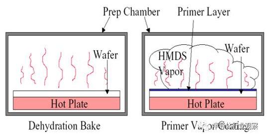
Pre-bake and primer vapor application
3.Photoresist Coating
The usual steps for photoresist coating are wet oxidation at 900-1100 degrees before coating the photoresist. The oxide layer can serve as a mask for wet etching or B implantation. As the first step in the photolithography process itself, a thin layer of an organic polymer compound that is sensitive to UV light, commonly known as photoresist, is applied to the sample surface (SiO2). First, the photoresist is taken out of the container and dropped onto the surface of the sample placed in the glue coating machine (the sample is fixed on the sample stage by vacuum negative pressure). The sample is then rotated at high speed, and the rotation speed is determined by the glue viscosity and the desired glue thickness. At such high speeds, the glue flows toward the edges under the action of centrifugal force.
Gluing processIt is the first and important step in the graphics conversion process. The quality of the glue directly affects the defect density of the processed device. In order to ensure the repeatability of the line width and the subsequent development time, the uniformity of the glue thickness of the same sample and the consistency of the glue thickness between different samples should not exceed ±5nm (for 1.5um glue thickness, it is ±0.3%).
The determination of the target thickness of the photoresist mainly considers the chemical properties of the resist itself and the fineness of the lines and gaps in the pattern to be copied. Glue that is too thick will result in edge coverage or connectivity, hilly or field-like glue appearance, and a decrease in yield. In MEMS, the glue thickness (after baking) is between 0.5-2um, and for special microstructure manufacturing, the glue thickness is sometimes expected to be on the order of 1cm. In the latter, spin coating will be replaced by methods such as cast glue or plasma glue polymerization. The optimization of the conventional photoresist coating process needs to consider the glue dripping speed, glue dripping amount, rotation speed, ambient temperature and humidity, etc. The stability of these factors is very important.
Let me talk here, the main components of photoresist are a polymer (resin), sensitizer and solvent. The structure of the polymer changes when it is irradiated, the solvent enables it to be ejected and a thin film is formed on the surface of the sample, and the sensitizer controls the chemical reaction of the polymeric phase. Photoresists that do not contain sensitizers are sometimes called unitary or one-component systems, while those containing sensitizers are called binary systems. Solvents or other additives are usually not included in the calculation because they do not directly participate in the photochemical reaction of the photoresist.
According to different properties, photoresists can be divided intoPositive glueandNegative glue。
In the early days of process development, negative glue has always dominated the photolithography process. With the emergence of VLSI IC and 2-5 micron pattern size, negative glue can no longer meet the requirements. Then positive glue appeared, but the disadvantage of positive glue is poor bonding ability.
Using positive glue requires changing the polarity of the mask, which is not a simple pattern flip. Because the mask is combined with two different photoresists, the sizes obtained by photolithography on the surface of the wafer are different. Due to the diffraction effect of light around the pattern, the pattern size obtained by combining the negative mask and the bright field mask on the photoresist layer is smaller than the pattern size on the mask. Using a combination of positive resist and darkfield mask will increase the size of the pattern on the photoresist layer.
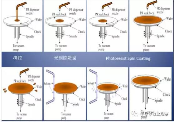
Photoresist coating
4.Soft Bake
After the photoresist is applied, a soft drying operation is required. This step is also called pre-baking. Pre-baking can evaporate the solvent in the photoresist and make the coated photoresist thinner.
In liquid photoresist, solvent components account for 65%-85%. Although the liquid photoresist has become a solid film after the glue is removed, there is still 10%-30% solvent, which is easily contaminated by dust. By baking at a higher temperature, the solvent can be evaporated from the photoresist (the solvent content is reduced to about 5% after pre-baking), thereby reducing dust contamination. At the same time, this step can also reduce the film stress caused by high-speed rotation, thereby improving the adhesion on the photoresist substrate.
During the pre-baking process, due to the volatilization of the solvent, the thickness of the photoresist will also be thinned. Generally, the thickness of the photoresist is about 10%-20%.
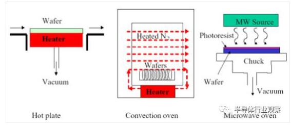
Baking Systems
5.Alignment
Photolithography alignment technology is an important step before exposure. As one of the three core technologies of photolithography, the alignment accuracy is generally required to be 1/7---1/10 of the smallest line width size. As the resolution of photolithography increases, the requirements for alignment accuracy are getting higher and higher. For example, for a 45am line width size, the alignment accuracy requirement is around 5am.
Driven by improvements in lithography resolution, alignment technology has also experienced rapid and diverse development. From the perspective of alignment principles and classification of mark structures, alignment technology has evolved from the early geometric imaging alignment methods in projection lithography, including video image alignment, binocular microscope alignment, etc., to the later zone plate alignment methods, interference intensity alignment, laser heterodyne interference, and moiré fringe alignment methods. From the perspective of alignment signals, it mainly includes marked microscopic image alignment, alignment based on light intensity information and alignment based on phase information.
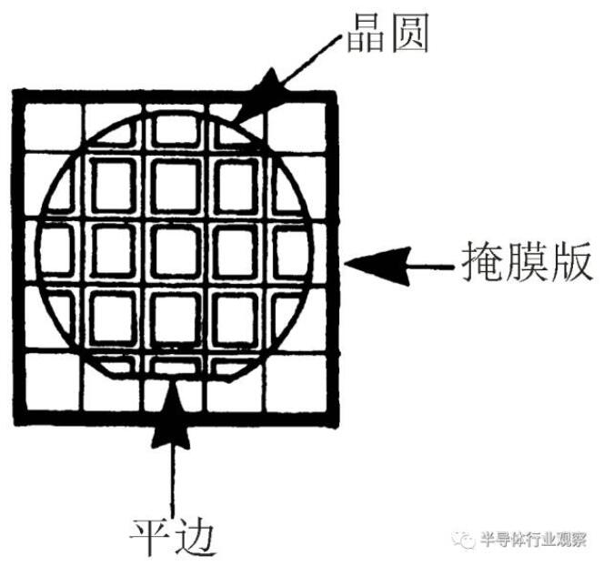
The alignment rule is that for the first photolithography, just make the Y axis on the mask 90º with the flat edge on the wafer, as shown in the figure. The subsequent masks are all aligned with the previous patterned mask using alignment marks. The alignment mark is a special pattern (see picture) distributed on the edge of each chip pattern. After the photolithography process, the alignment marks will remain on the chip surface forever and can be used for the next alignment.
Alignment methodinclude:
a. Pre-alignment, automatic laser alignment through notch or flat on the silicon wafer
b. Through the alignment mark, located on the cutting groove. In addition, inter-layer alignment, that is, overlay accuracy, ensures the alignment between graphics and existing graphics on the silicon wafer.
6.Exposure
In this step, the photoresist covering the substrate is selectively illuminated with light of a specific wavelength. The photosensitizer in the photoresist will undergo a photochemical reaction, causing the chemical composition of the area where the positive photoresist is illuminated (photosensitive area) and the area where the negative photoresist is not illuminated (non-photosensitive area) to change. These areas where the chemical composition has changed can be dissolved in a specific developer in the next step.
After being exposed to light, the photosensitive agent DQ in the positive photoresist undergoes a photochemical reaction and turns into ketene, which is further hydrolyzed into indene-Carboxylic-Acid (CA). The solubility of carboxylic acid in an alkaline solvent is about 100 times higher than that of the unsensitized part of the photoresist. The carboxylic acid produced also promotes the dissolution of the phenolic resin. By utilizing the different solubilities of photosensitive and non-photosensitive photoresists in alkaline solvents, the mask pattern can be transferred.
exposure methodinclude:
a. Contact printing (Contact Printing) mask is in direct contact with the photoresist layer.
b. Proximity Printing: The mask plate and the photoresist layer are slightly separated, about 10 to 50 μm.
c. Projection Printing. A lens is used between the mask and the photoresist to focus light to achieve exposure.
d. Stepper
Let me say something special hereprojection exposureClassification:
The two most important parameters in exposure are:
1. Exposure energy (Energy)
2.Focus
If the energy and focal length are not properly adjusted, graphics of the required resolution and size cannot be obtained. This indicates that the key dimensions of the graphic exceed the required range.
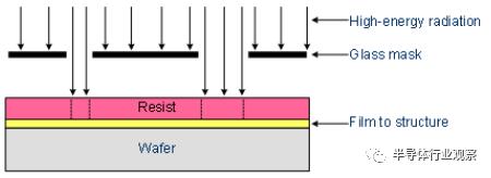
7.development
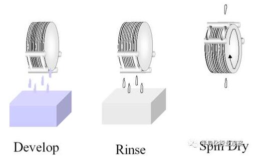
By adding the developer after the exposure process, the photosensitive areas of the positive photoresist and the non-photosensitive areas of the negative photoresist will be dissolved in the developer. After this step is completed, the pattern in the photoresist layer can be revealed. In order to improve the resolution, almost every kind of photoresist has a special developer to ensure high-quality development results.
The development process turns the recessive pattern formed during the exposure process into a dominant pattern with and without photoresist, which can be used as a mask for the next step of processing. What is carried out in development is the process of selective dissolution, and the most important thing is the ratio of the dissolution rate (DR) between the exposed area and the unexposed area. Commercial positive film has a DR ratio greater than 1000, a dissolution rate of 3000nm/min in the exposed area, and only a few nm/min in the unexposed area.
There are currently two developing methods, one iswet development, which is being widely used in IC and micromachining, the other isDry development。
a. Whole box silicon wafer immersion development (Batch Development).
Disadvantages: high developer consumption; poor uniformity of development;
b. Continuous Spray Development/Auto-rotation Development. One or more nozzles spray developer solution on the surface of the silicon wafer while the silicon wafer rotates at low speed (100 to 500 rpm). Nozzle spray pattern and wafer rotation speed are key tuning parameters to achieve repeatability of dissolution rate and uniformity from wafer to wafer.
c. Puddle (puddle development). Spray enough (but not too much, to minimize backside humidity) developer onto the wafer surface to form a puddle shape (keep the developer flow low to reduce edge development rate variations). The silicon wafer is fixed or rotated slowly. Generally, multiple spin coatings of the developer are used: apply for the first time, hold for 10 to 30 seconds, and remove; apply for the second time, hold, and remove. Then rinse with deionized water (to remove all chemicals from both sides of the wafer) and spin dry. Advantages: less developer dosage; uniform development of silicon wafer; minimized temperature gradient.
Developer:
a. Positive photoresist developer. The developer level of positive glue is alkaline aqueous solution. KOH and NaOH are generally not used in IC manufacturing because they will bring movable ion contamination (MIC, Movable Ion Contamination). The most common positive gel developer is tetramethylammonium hydroxide (TMAH) (standard equivalent concentration is 0.26, temperature 15~250C). Carboxylic acid is generated during I-line photoresist exposure. The alkali and acid in the TMAH developer neutralize the exposed photoresist in the developer, while the unexposed photoresist has no effect; the phenolic resin contained in chemical amplified photoresist (CAR, Chemical Amplified Resist) exists in the form of PHS. The acid generated by PAG in CAR will remove the protective group (t-BOC) in PHS, allowing PHS to quickly dissolve in the TMAH developer. During the entire development process, TMAH did not react with PHS.
b. Negative photoresist developer. xylene. The cleaning fluid is butyl acetate, ethanol, or trichlorethylene.
developingFAQ:
a. Incomplete Development. Photoresist remains on the surface. Caused by insufficient developer;
b. Under Development. The developed side walls are not vertical, caused by insufficient development time;
c. Over Development. The photoresist close to the surface is excessively dissolved by the developer, forming steps. Development time is too long.
8.Hard Bake
After the resist development is completed, the pattern is basically determined, but the properties of the photoresist need to be made more stable. This can be achieved by hard drying, a step also known as hardening. During this process, high-temperature treatment can be used to remove the remaining solvent in the photoresist, enhance the adhesion of the photoresist to the silicon wafer surface, and improve the etching resistance of the photoresist in subsequent etching and ion implantation processes. In addition, the photoresist will soften at high temperatures and form a molten state similar to that of glass at high temperatures. This will smoothen the photoresist surface under the action of surface tension and reduce defects (such as pinholes) in the photoresist layer, thus correcting the edge profile of the photoresist pattern.
The entire sample is treated with O2 plasma to remove possible unwanted residues after development, which is called de-scumming. Especially for negative glue but also positive glue, a thin layer of polymer will remain at the original glue-substrate interface after development. This problem is more serious in structures smaller than 1um or with large depth-to-width ratios. Of course, the remaining glue thickness will also decrease during the de-scumming process, but the impact will not be too great.
Finally, hard baking is required before etching or coating to remove residual developer and water, and annealing is required to improve the interface bonding condition due to penetration and expansion during the development process. At the same time, the hardness of the glue is increased and the etching resistance is improved. The hard baking temperature is generally as high as 120 degrees or more, and the time is about 20 minutes. The main limitation is that high temperatures can degrade pattern edges and make it difficult to remove after etching.
Method: Hot plate, 100~1300C (slightly higher than the glass transition temperature Tg), 1~2 minutes.
Purpose:
a. Completely evaporate the solvent in the photoresist (to avoid contaminating the subsequent ion implantation environment, for example, the nitrogen in the DNQ phenolic resin photoresist will cause local bursting of the photoresist);
b. Hard film to improve the ability of the photoresist to protect the lower surface during ion implantation or etching;
c. Further enhance the adhesion between the photoresist and the silicon wafer surface;
d. Further reduce the standing wave effect.
FAQ:
a. Underbake. Weaken the strength of the photoresist (resistance to etching and blocking ability in ion implantation); reduce Gapfill Capability for the needle hole; reduce adhesion to the substrate.
b. Overbake. It causes the flow of photoresist, which reduces the pattern accuracy and worsens the resolution. In addition, you can also use deep ultraviolet (DUV, Deep Ultra-Violet) to harden the film. The positive photoresist resin is cross-linked to form a thin surface hard shell, which increases the thermal stability of the photoresist. In the subsequent plasma etching and ion implantation (125~2000C) processes, the reduction in resolution caused by high-temperature flow of photoresist is reduced.
9.Etching or ion implantation
Etching is a process in semiconductor device manufacturing that uses chemical means to selectively remove specific parts of a deposited layer. Etching is very important for the electrical performance of the device. If errors occur during the etching process, the silicon wafer will be scrapped and will be difficult to recover, so strict process control must be carried out. Each layer of a semiconductor device undergoes multiple etching steps.
Etching is generally divided into electron beam etching and photolithography. Photolithography has high requirements on the flatness of the material, so it requires a high degree of cleanliness. However, for electron beam etching, because the wavelength of electrons is extremely short, the resolution is much better than that of photolithography. Because no mask is required, the flatness requirements are not high, but electron beam etching is slow and the equipment is expensive.
For most etching steps, portions of the upper layer of the wafer are protected by a "mask" that cannot be etched, allowing specific portions of the layer to be selectively removed. In some cases, the material of the mask is photoresistive, which is similar to the principle used in photolithography. In other cases, the etching mask needs to be resistant to certain chemicals, and silicon nitride can be used to create such a "mask."
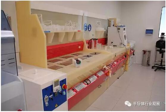
Ion implantation is a technical method that accelerates specific ions in an electric field and then embeds them into another solid material. Using this technology can change the physical and chemical properties of solid materials, and it has now been widely used in semiconductor device manufacturing and certain materials research. Ion implantation can cause nuclear transformations, or change the crystal structure of some solid materials.
10.Photoresist removal
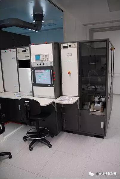
The main function of the photoresist is to protect the portion of the substrate underneath the photoresist while the entire area is undergoing chemical or mechanical processing processes. Therefore, when the above process is completed, the photoresist should be completely removed. This step is referred to as glue removal. Only those photoresists that are stable at high temperatures, such as light-sensitive polyimides, can be left on the device as an intermediary or buffer coating.
To avoid any damage to the surface being treated, mild chemical methods at low temperatures should be used. The application of ultrasonic waves can also enhance peeling performance. Some known stripping solutions cannot work on metal surfaces such as aluminum because of corrosion problems; in this case, ozone or oxygen plasma (ashing) is used first. These plasmas are also successful as photolithography strippers for non-aluminum surfaces, however, damage to the device surface is still an issue to be addressed.
After etching or ion implantation, the photoresist is no longer needed as a protective layer and can be removed. The methods of removing glue are classified as follows:
Wet glue removal
Organic solvent removal: Use organic solvents to remove photoresist
Inorganic solvent: By using some inorganic solvents, the carbon element in the photoresist, an organic matter, is oxidized into carbon dioxide and then removed.
Dry photoresist stripping: using plasma to remove photoresist
In addition to these main processes, some auxiliary processes are often used, such as uniform etching over a large area to reduce the thickness of the substrate, or the process of removing edge unevenness, etc. Generally, when producing semiconductor chips or other components, a substrate needs to be photolithographed multiple times.
The above are the steps of photolithography. I hereby collect them for everyone. I hope you can correct me.
Disclaimer: This article is reproduced from "Semiconductor Industry Observation". This article only represents the author's personal views and does not represent the views of Sacco Micro and the industry. It is only for reprinting and sharing to support the protection of intellectual property rights. Please indicate the original source and author for reprinting. If there is any infringement, please contact us to delete it.
Company phone number: +86-0755-83044319
Fax/FAX: +86-0755-83975897
Email: 1615456225@qq.com
QQ: 3518641314 Manager Li
QQ: 332496225 Manager Qiu
Address: Room 809, Building C, Zhantao Technology Building, No. 1079 Minzhi Avenue, Longhua New District, Shenzhen
Related Recommendations
Exclusive Interview with Li Gang of Yunfan Ruida: The Precision of Millimeter-Wave Radar Products and the Warmth of Humanity
2026-07-22
2523
RF Passion, Craftsman’s Journey: Over 30 Years of Steadfast Dedication — Interview with Kinghelm Chief Engineer Mr. Qin hongxiang
2026-06-26
2689





 粤公网安备44030002007346号