
























Service Hotline
News

News
A discussion on the development trends of advanced semiconductor manufacturing equipment and the status of equipment autonomy
2022-03-17
862
Semiconductors have entered the atomic level processing level. Manufacturing semiconductor devices at this precision requires the integration of knowledge and technology from more than 50 disciplines. Moreover, processing accuracy is only one dimension. Yield is vital to semiconductor manufacturing. Therefore, uniformity, stability, repeatability, reliability and cleanliness are all important. There are more than 1,000 advanced semiconductor processing links. If there is a problem in any link, it will be difficult to manufacture chips that meet product performance and yield requirements.
According to statistics from market research organization SEMI, mainland China became the world's largest regional market for semiconductor equipment for the first time in 2020, with sales increasing by 39% year-on-year to US$18.72 billion; Taiwan ranked second, with equipment manufacturers' sales in Taiwan reaching US$17.15 billion in 2020; South Korea ranked third, with sales increasing 61% year-on-year to US$16.08 billion; Japan ranked fourth, with sales also reaching US$7.58 billion. East Asia has become the highland of the global semiconductor arms race, spending a total of US$59.53 billion in 2020, accounting for 83.6% of the total global semiconductor equipment expenditure (US$71.2 billion) that year. (Warm reminder: For information related to semiconductor equipment, please go to the backend to reply [Semiconductor equipment】receive)
Due to the intensified impact of geopolitics on the semiconductor supply chain, competition for semiconductor production capacity investment in various regional markets will become fierce in 2021. TSMC and Samsung have both adjusted their capital expenditure plans for semiconductors in 2021 to more than US$30 billion. The two companies are desperately competing on the progress of mass production of advanced processes. Both expect to mass produce 3-nanometer processes in 2022. At the call of the US government, TSMC and Samsung will also set up factories in the United States. There is no doubt that 2021 will be another bumper year for semiconductor equipment manufacturers. However, due to relevant restrictions, mainland China is unable to purchase high-end EUV lithography machines and other equipment, and it may be difficult to maintain its position as the largest equipment market.
According to the Taiwan Industrial Technology Research Institute (hereinafter referred to as Taiwan Industrial Technology Research Institute), different regional markets have different goals for the development of the semiconductor industry: As the world's largest semiconductor application market, mainland China undoubtedly hopes to speed up technological catch-up in the context of threats to supply chain security to alleviate the current situation of being controlled by others in key links such as manufacturing, equipment and materials; and the United States, as the leader of the global semiconductor industry chain , will continue to strengthen the export control of high-end chip manufacturing equipment to mainland China, and the United States will also introduce new policies to deal with the decline in U.S. wafer manufacturing capacity in recent years; as the two regions with the highest wafer manufacturing density in the world, Taiwan and South Korea are expected to continue to lead the development trend of wafer manufacturing processes. These two regions will also use their strong manufacturing capabilities to improve upstream materials and equipment independence.
Advanced technology development direction
After 28 nanometers, the planar transistor process reached its limit, and FinFET (fin transistor) continued Moore's Law, pushing the process node to below the current 10 nanometers. However, the FinFET route is approaching its limit. Samsung will be the first to adopt the GAA (gate all around) structure on the 3nm process, while TSMC will continue the FinFET structure at the 3nm node and then adopt the GAA structure at the 2nm node. Taiwan's Industrial Technology Research Institute believes that Intel has encountered trouble in wafer manufacturing. The 7-nanometer process (note: the three companies have different definitions of process size and are not suitable for direct numerical comparison) may be delayed until 2023 before mass production. It is expected that Intel will also change to the GAA architecture at the 5-nanometer node.
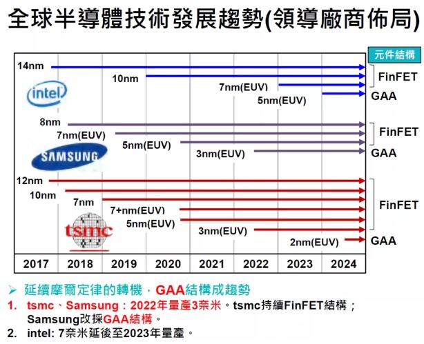
Source: Taiwan Industrial Technology Research Institute
GAA, the full name of Gate-All-Around, is a wrap-around gate technology transistor, also called GAAFET. The concept was proposed very early, in an article published by Dr. Cor Claeys and his research team at IMEC in Belgium in 1990. GAAFET is equivalent to an improved version of 3D FinFET. The transistor structure under this technology has changed again. The gate and drain are no longer fins, but become "little sticks" that pass vertically through the gate. In this way, the gate can wrap the source and drain on all sides.
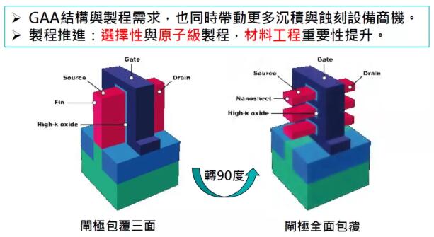
Source: Taiwan Industrial Technology Research Institute
Compared with FinFET, the original source and drain semiconductors were fins (Fin), but now the gate has become a fin. Therefore, GAAFET and 3D FinFET have many similarities in their implementation principles and ideas - which is a great advantage for fabs. From three contact surfaces to four contact surfaces, and also split into several four contact surfaces, it is obvious that the gate's ability to control the current has been further improved.
Compared with the FinFET process, the GAA structure has a larger gate contact area, which improves the transistor's ability to control the conductive channel and significantly improves parasitic parameters such as capacitance. Therefore, it can reduce the operating voltage, reduce leakage current, reduce power consumption and operating temperature, which is conducive to increasing integration and continuing Moore's Law.
Since the production process required for the new structure is similar to that of fin transistors, the key process steps are almost the same, and existing equipment and technological achievements can be continued to be used. For TSMC and Samsung, this is undoubtedly the lowest-cost technology route replacement solution. However, GAA's requirements for processing accuracy have further increased, requiring regional selective deposition technology and atomic-level processing capabilities. Therefore, the increased importance of materials engineering will also drive more business opportunities for deposition and etching equipment.
The semiconductor front-end equipment market controlled by the five giants
Although more than 80% of the world's equipment will be sold to East Asia in 2020, apart from Japan, China (Mainland plus Taiwan) and South Korea do not have much influence in the equipment industry. The world's top five semiconductor front-end (ie wafer manufacturing, packaging is the back-end) equipment manufacturers Applied Materials (AMAT), ASML (ASML), Lam (Lam), Tokyo Electronics (TEL) and KLA (KLA) account for more than 70% of the market share. Among them, only Tokyo Electronics is headquartered in East Asia, and the rest are American and European companies.
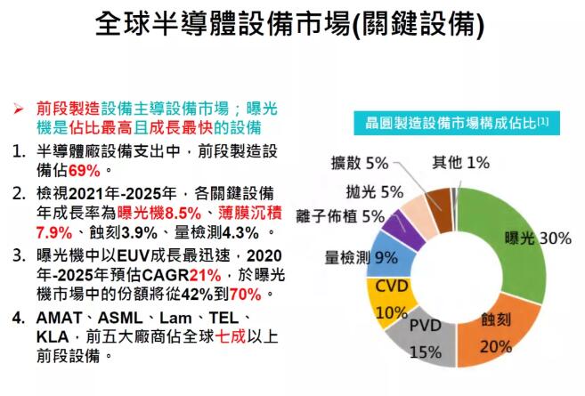
Source: Taiwan Industrial Technology Research Institute
Specifically, Applied Materials ranked first. Its revenue in 2020 was US$17.2 billion, of which the semiconductor business accounted for about 70%. Applied Materials has a wide range of semiconductor equipment, including PVD (thin film deposition) equipment accounting for 38% of the world, CMP (grinding and polishing) equipment accounting for 70%, etching equipment accounting for 15%, and ion implanters accounting for 67%.
ASML ranks second, with revenue of 13.98 billion euros in 2020. ASML is a major manufacturer of lithography machines, and it is currently the only supplier in the world of EUV (extreme ultraviolet) lithography machines. Thanks to TSMC, Samsung and Intel's pursuit of advanced processes, ASML sold 31 EUV lithography machines in 2020, totaling 4.5 billion euros. These 31 EUV lithography machines alone accounted for 32% of its total revenue. Currently, ASML is working with supply chain partners to jointly develop more sophisticated lithography processing technology. For example, it will launch multiple electron beam detection and scanning systems in 2020, and limit the interference between electron beams to less than 2%, which is suitable for processes above the 5-nanometer node. ASML is also cooperating with Lam and imec to develop dry photoresist technology to improve EUV resolution and reduce the amount of photoresist. It also cooperates with Lasertec to develop a new generation of EUV mask inspection technology to reduce costs, and cooperates with TSMC to develop a new generation of EUV mask cleaning technology to reduce costs.
Tokyo Electronics' equipment sales in 2020 were US$10.37 billion, ranking third. Tokyo Electronics' market share of coating and developing equipment accounts for 91% of the global market share, among which EUV coating and developing machines account for the entire market share, etching machines account for 25% of the world, deposition equipment accounts for 37%, and cleaning equipment accounts for 27%. From 2020 to 2022, Tokyo Electronics plans to invest 400 billion yen in R&D funds, focusing on selective deposition, smart etching, supercritical fluid cleaning and other technical directions.
Lam Semiconductor's revenue in 2020 was US$10.05 billion, ranking fourth. Lam is the world's leader in etching equipment, with its memory manufacturing business accounting for 57% and logic technology accounting for 43%. It is the only company among the top five equipment manufacturers whose memory business accounts for more than 50%. As mentioned earlier, Lam and ASML are working with imec to develop EUV dry photoresist technology.
Kelei Semiconductor's revenue in 2020 was US$5.81 billion, ranking fifth. Kelei is the world leader in wafer inspection equipment, accounting for more than 50% of the market share. Kelei also invests in the development of electron beam defect measurement technology for structures smaller than 5 nanometers in stress deformation measurement and multi-beam inspection.
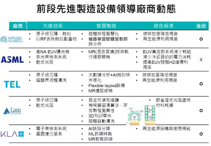
Source: Taiwan Industrial Technology Research Institute
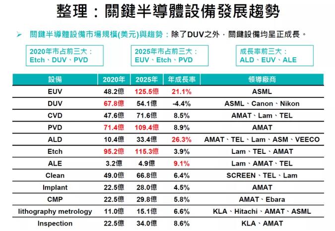
According to estimates from Taiwan's Industrial Research Institute, the world's key semiconductor equipment will have a very good growth momentum in the next few years. Except for DUV (deep ultraviolet) lithography equipment, other equipment will show positive growth. Among them, ALD (atomic layer deposition) has the highest growth rate, with an average annual growth rate of 26.3% expected from 2020 to 2025. EUV equipment ranks second in growth rate, with an average annual growth rate of double digits. EUV equipment ranks first in terms of value. Sales of EUV equipment are expected to reach US$12.55 billion in 2025, surpassing etching machines and becoming the semiconductor equipment with the highest sales in each segment.
Source: Taiwan Industrial Technology Research Institute
Chinese equipment manufacturers have a long way to go
Compared with international manufacturers, there is a big gap between Chinese equipment manufacturers in terms of sales scale and technology. According to data from the Electronic Special Equipment Industry Association, the sales of domestic semiconductor equipment in 2019 was 16.182 billion yuan, which was only about half of the revenue of the top five gatekeepers Kelei in 2019 (US$4.6 billion). The association estimated in October 2020 that the sales of domestic semiconductor equipment in 2020 would total 21.3 billion yuan, which is still less than 60% of that of Kelei (US$5.8 billion).
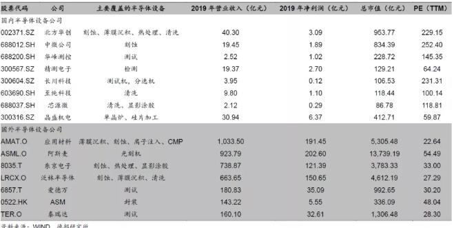
Comparison of major domestic and foreign semiconductor equipment companies (as of January 6, 2021)
Source: Deppon Securities
Technically, my country's semiconductor equipment has basically not yet participated in the research and development stage of advanced processes (3 nanometers and below), and it is currently unable to support the national production of quasi-mainstream processes such as 28 nanometers. Most domestic equipment manufacturers' commercial products are still based on mature process production lines. Taking the lithography machine that attracts high social attention as an example, domestically it is mainly Shanghai Microelectronics Equipment Co., Ltd. (referred to as "Shanghai Microelectronics"). Shanghai Microelectronics' mainstream products can only meet the lithography process requirements of 90 nanometer, 110 nanometer and other processes.
But there are also some fields that have already participated in the advanced technology competition. For example, China Micro Semiconductor has been recognized by TSMC in the field of CCP etching and has entered its 7nm/5nm production line; Northern Huachuang is relatively outstanding in ICP etching equipment, and etching equipment above 28nm has been industrialized. In terms of advanced processes, silicon etching equipment has broken through 14nm technology and entered the Shanghai Integrated Circuit R&D Center.
According to the "Made in China 2025" goal, semiconductor core basic components and key basic materials should achieve a 40% autonomy rate in 2020, and a 70% localization rate in 2025. However, according to the public bidding information of ten domestic wafer manufacturing companies such as Yangtze Memory and Huali Microelectronics from 2017 to the first quarter of 2021, the localization rate is still far from the target. From 2017 to 2019, these ten manufacturers opened bids for a total of 4,197 equipment, of which 431 were Chinese-made equipment, with a localization rate of approximately 10.3%. From 2020 to the first quarter of 2021, these ten fabs opened bids for a total of 1,862 equipment, of which 315 were Chinese-made equipment. It is estimated that the current localization rate is 17%, an increase of more than 6 percentage points from 2017 to 2019.
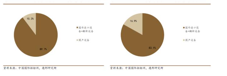
Left: Localization rate of top ten wafer fab equipment from 2017 to 2019
Right: Localization rate of equipment in the top ten wafer fabs in the first quarter of 2020-2021
Source: Deppon Securities
However, domestic semiconductor equipment has also shown very positive changes in the past few years. In terms of technology, companies led by China Micro Semiconductor, Northern Huachuang and Yitang Semiconductor are already close to the world's first-class manufacturers in the fields of etching, deposition, dry stripping, cleaning, and ion implantation. In terms of market share, the market share of some products has exceeded 20%, which has launched a strong impact on the market position of international semiconductor equipment manufacturers.
It can be seen from the bidding information released by the top ten wafer fabs that from 2017 to the first quarter of 2021, the localization rate of dry degumming equipment reached 45.5%, while the localization rates of cleaning equipment (30.6%), etching equipment (22.2%), and polishing equipment (21.6%) were all higher than 20%, and furnace tube equipment (14.7%) %) and glue development equipment (10.0%) are both higher than 10%. The localization rate of deposition equipment (8.5%) and front-end testing equipment (5.2%) is relatively low, only between 5% and 10%. The biggest gaps are ion implanters (2.4%), back-end testing equipment (1.9%) and photolithography machines (1.6%).
After entering 2020, the localization rate will increase faster. Judging from the bid opening data of the top ten wafer fabs, in the first quarter of 2020 to 2021, the localization rate of polishing equipment, etching equipment, furnace tube equipment and glue coating and development equipment all increased by more than double digits compared with the localization rate in the 2017 to 2019 stage.
Judging from the development trend of the global semiconductor equipment industry, as the semiconductor process approaches the physical limit, it becomes increasingly difficult to develop a new generation of equipment. Taking EUV lithography machines as an example, the project was initiated as early as the 1990s. Nearly 200 research institutions from more than 40 countries around the world (Europe contributed more than 100) participated in it. From basic research, technical research to system integration, the entire R&D system invested more than 100 billion yuan, exceeding the total revenue of my country's equipment industry in the past ten years.
Yin Zhiyao, chairman of China Microelectronics Semiconductor, also said in an interview with the media that semiconductors have entered the atomic level processing level. Manufacturing semiconductor devices at this precision requires the integration of knowledge and technology from more than 50 disciplines. He pointed out that plasma etching has carved pores that are one thousandth to one hundred thousandth the diameter of a human hair, and the accuracy, uniformity and repeatability of the hole diameter can reach tens of thousands to one hundred thousandth the diameter of a human hair. An etching machine processes more than one million trillion thin and deep contact holes every year, and almost 100% of the holes must be completely opened.
Semiconductor equipment must not only be able to achieve very fine processing, but the most important things are uniformity, stability, repeatability, reliability and cleanliness. Only by doing this can we meet the core requirement of wafer manufacturing, which is chip qualification rate. To ensure an acceptable pass rate (for example, 90%), each processing and manufacturing link requires an extremely high pass rate, because currently advanced process chips require 1,000 process steps. If the pass rate of each step is 99.9%, the final pass rate after 1,000 steps is only 36.77%.
As a representative of modern intelligent manufacturing and the underlying support of the global information industry, chip manufacturing rarely gives new equipment manufacturers the opportunity to try and make mistakes. After all the hard work to develop the prototype, only a small part of the development and production equipment has been completed. The more difficult part is to convince the wafer manufacturer to help with the test run at the risk of a decrease in qualification rate and production capacity. Yin Zhiyao said that after the prototype is made and the customer is willing to cooperate, it must pass at least 80 rigorous test items to finally meet the requirements of the wafer fab.
Judging from the historical development experience of international manufacturers, the equipment industry must stabilize the market and not make any rash advances. It must invest in long-term research and development and consolidate its technical foundation. As Yin Zhiyao said, semiconductor equipment requires the collaboration of 50 disciplines, which is no less difficult than two bombs and one satellite. "Only two or three companies in the world can make the magnetically levitated molecular pump, one of the key core components of the semiconductor industry. Everything requires long-term technology accumulation."
Thanks to globalization, the semiconductor industry has developed to its current scale. However, since the Trump administration came to power, the United States has used the semiconductor industry as a weapon to launch a technological war against China, which has seriously affected the supply chain mutual trust mechanism previously established by the global electronic information industry. As the world's most important electronic information industry manufacturing base, it is crucial to create a new semiconductor supply chain that is not affected by geopolitics. Whenever a technology truly achieves a real market breakthrough (for example, the market share reaches 20%), the corresponding restrictions in the Wassenaar Agreement lose their meaning. At present, whether the localization rate of equipment can be effectively improved has become a key factor in the healthy development of the global electronic information industry. China's rapid expansion in wafer manufacturing has provided domestic semiconductor equipment manufacturers with broad market space and trial and error opportunities. For domestic semiconductor equipment manufacturers, this is an excellent historical opportunity.
Disclaimer: This article is reprinted from "TechSugar". This article only represents the author's personal views and does not represent the views of Sacco Micro and the industry. It is only for reprinting and sharing to support the protection of intellectual property rights. Please indicate the original source and author for reprinting. If there is any infringement, please contact us to delete it.
Company phone number: +86-0755-83044319
Fax/FAX: +86-0755-83975897
Email: 1615456225@qq.com
QQ: 3518641314 Manager Li
QQ: 332496225 Manager Qiu
Address: Room 809, Building C, Zhantao Technology Building, No. 1079 Minzhi Avenue, Longhua New District, Shenzhen
Related Recommendations
Exclusive Interview with Li Gang of Yunfan Ruida: The Precision of Millimeter-Wave Radar Products and the Warmth of Humanity
2026-07-22
2541
RF Passion, Craftsman’s Journey: Over 30 Years of Steadfast Dedication — Interview with Kinghelm Chief Engineer Mr. Qin hongxiang
2026-06-26
2704





 粤公网安备44030002007346号