
























Service Hotline
News

News
Electronic analysis of the reliability and applications of SiC power devices
2022-03-17
812
As a third-generation semiconductor material, SiC has superior performance to Si-based materials in all aspects. Compared with traditional power devices based on Si semiconductor materials, emerging SiC power devices have the advantages of fast switching speed, high blocking voltage and strong high-temperature working ability, and can better meet the development requirements of future power electronics technology.
Shanghai Zhanxin Electronics After three years of in-depth research and development and hard work, it has become the first company in China to master 6-inch SiC MOSFET and SBD processes, as well as SiC MOSFET driver chips. This article explains the reliability and application of Zhanxin Electronics' SiC power devices, so that users can rest assured before use and worry during use, thereby making better products.
1. Does Shanghai Zhanxin Electronics’ SiC MOSFET have data on the positive and negative voltage stress limits?
Zhanxin Electronics' SiC MOSFET gate voltage specification (+20V/-5V) is strictly certified in accordance with JEDEC, ensuring that the product's working life is not less than 10 years at room temperature. For applications that exceed the gate voltage specification, there are two main considerations.
First, the lifetime model of the gate itself is mainly determined by the TDDB (Time Dependent Dielectric Breakdown) model of SiO2. There is already a large amount of data showing that the quality of the SiO2 dielectric layer grown on SiC is as good as the SiO2 grown on Si. Therefore, from the perspective of TDDB, the higher voltage that the 20V gate dielectric can withstand and the life model at this voltage are similar to those of Si. MOSFET and IGBT are the same; Zhanxin Electronics is using Zhanxin’s own SiC MOSFET to establish the SiO2 gate dielectric process and device life model.
Second, the biggest difference and challenge between SiC MOSFET and Si MOS products (MOSFET and IGBT) is PBTI (Positive Bias Temperature Instability) and NBTI (Negative Bias Temperature) Instability (negative bias temperature instability), the Vth of the device will increase after adding positive bias, and the Vth of the device will decrease after adding negative bias; under JEDEC certification conditions, the life of the device can be guaranteed by operating within the gate voltage specification; for application life models that exceed the gate voltage specification, Zhanxin Electronics is building equipment and doing detailed planning and research; generally speaking, as long as the positive gate voltage does not exceed 25V and the negative gate voltage does not fall below -10V, DutyCycle's relatively small pulses will not cause unrecoverable damage to the device's performance. The specific quantitative relationship and life model will be given at the end of the first round of research.
2. How does Shanghai Zhanxin Electronics solve the problem of establishing negative driving voltage in SiC MOSFET applications? Is this approach reliable?
Zhanxin Electronics has developed the industry's first 35V/4A driver IVCR1401D/IVCR1401DP in an 8-pin package with integrated negative voltage drive. After the driver starts, the NEG output is pulled to GND, and the internal current source quickly charges the negative voltage capacitor. After the negative voltage is established, the NEG pin is released, and the internal negative voltage regulator can adjust the negative voltage to -3.5V for normal operation. After that, the gate drive signal NEG switches between (VCC-3.5V) and -3.5. The figure below shows the negative voltage establishment process of the negative voltage capacitor. It takes about 28us to charge a 1uF capacitor. X7R capacitors with more than 100 times Cg capacitance should be used to reduce the ripple on the negative voltage capacitor, so that the negative voltage can be established and driven reliably and stably. Our company's aging test system circuit has been verified using this chip. It can drive SiC MOSFET under the operating conditions of 1000V/20A/125℃. After continuous operation for 1000h, it can still be driven stably and reliably.
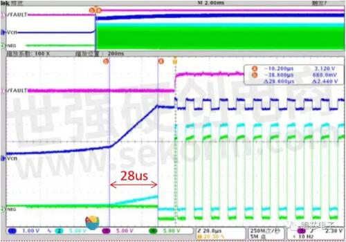 图 1 3. How does Shanghai Zhanxin Electronics solve the problem of negative voltage spikes in SiC MOSFET applications? What is the mechanism of negative pressure spike generation? What are the ways to deal with it?
SiC MOSFET has faster switching speed than traditional Si power devices. However, this fast transient process will make the switching performance of SiC MOSFET more sensitive to the parasitic parameters of the loop, especially reflected in the drive waveform. The figure below shows the voltage spike produced by the Miller effect. In SiC In the half-bridge application of MOSFET, the lower tube remains off. When the upper tube is turned off, a larger dv/dt will be generated. Due to the parasitic inductance in the power loop and drive loop, a larger Miller current will be generated. This current will generate a voltage drop on the drive resistor RG, resulting in VGS A negative spike appears on the waveform; similarly, when the upper tube is turned on, a larger dv/dt will also be generated. Due to the parasitic inductance present in the loop, a larger Miller current will also be generated. This current will generate a voltage drop on the drive resistor RG, resulting in a positive spike appearing on the VGS waveform.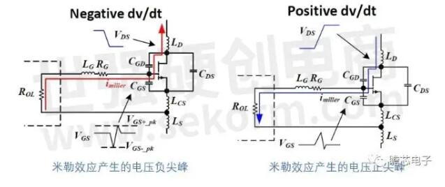 图 2
图 2
In order to reduce the negative pressure spike of the drive, there are several suggestions:
1) Connect a back-to-back MOS (recommended model: QS5K2TR) in parallel to the driving resistor RG to reduce the voltage drop caused by the Miller effect on RG, thereby reducing the Miller peak voltage, as shown in the figure below Q1, Q2;
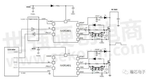 Figure 3 2) Place the driver chip as close as possible to the gate of the SiC MOSFET to reduce the parasitic inductance in the drive loop as much as possible; 3) Minimize the area of the power loop in the layout, and minimize the common source inductance in the power loop and the drive loop; 4) When conditions permit, use TO247-4 packaged SiC MOSFET, and use Kelvin drive as much as possible to reduce the parasitic inductance caused by the device pins.
4. How does Shanghai Zhanxin Electronics solve the switching oscillation problem in SiC MOSFET applications?
The most critical thing about the SiC MOSFET oscillation problem is to first solve the drive circuit oscillation problem and prevent oscillation caused by the oscillation of the drive signal. In order to solve the problem of drive loop oscillation, the drive chip needs to be placed as close as possible to the gate of the SiC MOSFET to reduce parasitic inductance and oscillation as much as possible. There are two pictures below. The upper picture shows the test waveform when the driver chip is far away from the SiCMOSFET, and the lower picture shows the test waveform when it is closer. The sky blue waveform in the two figures is the Vgs waveform, and the yellow is the Vds waveform. In the left picture, the Miller peak is as high as 19.2V, while in the right picture, the Miller peak is only 4.6V. The main reason for such a big improvement is that the driver IC is relatively close to the SiC MOSFET.
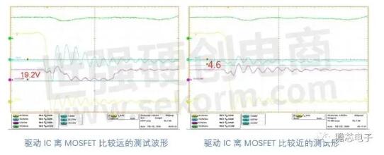 图 4
图 4
Next, we will explain some points to note about the layout of SiC MOSFET. A good layout will help reduce oscillation. First, the driver IC should be as close as possible to the SiC MOSFET to ensure that the driver circuit area is as small as possible. Secondly, high-frequency oscillation is caused by the oscillation between the PCB and the stray inductance and stray capacitance (mainly Coss) of the MOSFET. As shown in the figure below, the red dotted line is the area of the power loop, and the green dotted line is the area of the drive loop. The smaller these areas are, the smaller the oscillation when the SiC MOSFET switches.
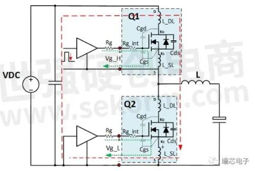 图 5
5. What are the similarities and differences between SiC MOSFET driver and Si IGBT driver? Can SiC MOSFET be driven using the IGBT plug-in driver board method?
图 5
5. What are the similarities and differences between SiC MOSFET driver and Si IGBT driver? Can SiC MOSFET be driven using the IGBT plug-in driver board method?
Cannot be used. Because the drive board is used, the parasitic inductance of the drive circuit is relatively large, which requires a larger drive resistor for damping, which in turn causes the switching speed to slow down and the loss to increase. If a larger drive resistor is not used for damping, the Vgs waveform will cause a relatively large oscillation, which will lead to Vds oscillation, thereby increasing switching losses. In addition, the relatively large parasitic inductance itself increases the impedance of the driving circuit, and the anti-Miller ability of the driving circuit is weakened, resulting in slower switching speed and increased loss.
6. What should we pay attention to when connecting SiC MOSFETs in parallel?
To ensure that the drive circuit of each SiC MOSFET and the main power circuit are as symmetrical as possible, the distance from the driver chip output to the gate of each SiC MOSFET is required to be the same. MOSFETs require a separate Rg to increase consistency. If parallel MOSFETs share a driving resistor, the MOSFET with the smallest threshold voltage will be turned on first, and the Vgs of other MOSFETs will be clamped at the threshold voltage, resulting in only the MOSFET with the smallest threshold voltage being turned on, and all other tubes not being turned on. The same is true for the turn-off process. The MOSFET with the highest threshold voltage is turned off first, and the voltage is clamped at the threshold voltage until the MOSFET completes the turn-off process. It can be seen that using one driving resistor to drive all MOSFETs will cause relatively large dynamic uneven current flow at switching instants. For this purpose, a separate Rg needs to be configured for each MOSFET, so that the Vgs of each MOSFET is decoupled and dynamic current sharing is enhanced. The static current sharing characteristics are mainly achieved by the parameter consistency of the MOSFET itself. MOSFETs with consistent parameters need to be carefully selected for direct parallel connection.
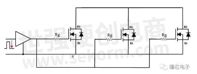 图 6
图 6
8. How much better is the parasitic inductance of SiC MOSFET TO247-4 than TO247-3? Are there any specific parameters?
According to data published by CREE, the switching loss of the TO247-4 package is only 30% of the switching loss of the TO247-3 package (600V/40A). It can be seen that the advantages of TO247-4 packaging are very obvious.
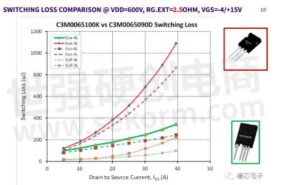 图 7
图 7
The internal common Source inductor inside the TO247-3 package will slow down the turn-on and turn-off speed of the MOSFET, thereby increasing the switching loss. However, the TO247-4 has a separate Source lead for driving, thereby bypassing the internal common Source inductor and avoiding the impact of the internal common Source inductor on the switching process, thus achieving the purpose of reducing switching losses. First, let’s look at the turn-on process. In a typical double-pulse experiment, it is achieved by switching the upper tube on and off. We mainly focus on the upper tube Vgs loop. When the upper tube is turned on, the Id of Q1 increases, then the voltage induced by L_SL is positive up and negative down, and its voltage has the same polarity as the external driving voltage (positive voltage), which causes the Vgs voltage on the internal MOSFET-Die to decrease, thus slowing down the MOSFET turn-on process.
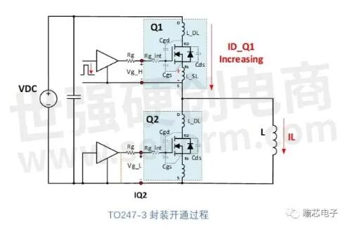 图 8
图 8
Next, let’s look at the turn-off process of the upper tube. Q1 turns off, causing Id to decrease. The voltage induced by L_SL is negative at the top and positive at the bottom. This voltage has the opposite polarity to the external drive voltage (negative voltage or zero voltage), which will reduce the voltage of Vgs on the actual internal MOSFET-Die during the turn-off process. If the voltage on L_SL is large enough, it can even cause the voltage on the internal MOSFET-Die to change from negative to positive, leading to mistaken turn-on! So L_SL will cause the turn-off process to slow down, thereby increasing the turn-off loss.
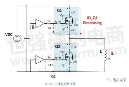 图 9
图 9
The figure below uses a TO247-4 package. Because there is a separate Kelvin-Source lead, the induced voltage on L_SL cannot affect the drive circuit, thereby increasing the switching speed and reducing switching losses.
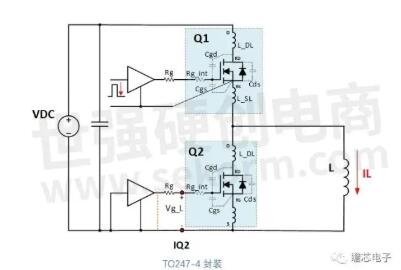
Shanghai Zhanxin Electronics After three years of in-depth research and development and hard work, it has become the first company in China to master 6-inch SiC MOSFET and SBD processes, as well as SiC MOSFET driver chips. This article explains the reliability and application of Zhanxin Electronics' SiC power devices, so that users can rest assured before use and worry during use, thereby making better products.
1. Does Shanghai Zhanxin Electronics’ SiC MOSFET have data on the positive and negative voltage stress limits?
Zhanxin Electronics' SiC MOSFET gate voltage specification (+20V/-5V) is strictly certified in accordance with JEDEC, ensuring that the product's working life is not less than 10 years at room temperature. For applications that exceed the gate voltage specification, there are two main considerations.
First, the lifetime model of the gate itself is mainly determined by the TDDB (Time Dependent Dielectric Breakdown) model of SiO2. There is already a large amount of data showing that the quality of the SiO2 dielectric layer grown on SiC is as good as the SiO2 grown on Si. Therefore, from the perspective of TDDB, the higher voltage that the 20V gate dielectric can withstand and the life model at this voltage are similar to those of Si. MOSFET and IGBT are the same; Zhanxin Electronics is using Zhanxin’s own SiC MOSFET to establish the SiO2 gate dielectric process and device life model.
Second, the biggest difference and challenge between SiC MOSFET and Si MOS products (MOSFET and IGBT) is PBTI (Positive Bias Temperature Instability) and NBTI (Negative Bias Temperature) Instability (negative bias temperature instability), the Vth of the device will increase after adding positive bias, and the Vth of the device will decrease after adding negative bias; under JEDEC certification conditions, the life of the device can be guaranteed by operating within the gate voltage specification; for application life models that exceed the gate voltage specification, Zhanxin Electronics is building equipment and doing detailed planning and research; generally speaking, as long as the positive gate voltage does not exceed 25V and the negative gate voltage does not fall below -10V, DutyCycle's relatively small pulses will not cause unrecoverable damage to the device's performance. The specific quantitative relationship and life model will be given at the end of the first round of research.
2. How does Shanghai Zhanxin Electronics solve the problem of establishing negative driving voltage in SiC MOSFET applications? Is this approach reliable?
Zhanxin Electronics has developed the industry's first 35V/4A driver IVCR1401D/IVCR1401DP in an 8-pin package with integrated negative voltage drive. After the driver starts, the NEG output is pulled to GND, and the internal current source quickly charges the negative voltage capacitor. After the negative voltage is established, the NEG pin is released, and the internal negative voltage regulator can adjust the negative voltage to -3.5V for normal operation. After that, the gate drive signal NEG switches between (VCC-3.5V) and -3.5. The figure below shows the negative voltage establishment process of the negative voltage capacitor. It takes about 28us to charge a 1uF capacitor. X7R capacitors with more than 100 times Cg capacitance should be used to reduce the ripple on the negative voltage capacitor, so that the negative voltage can be established and driven reliably and stably. Our company's aging test system circuit has been verified using this chip. It can drive SiC MOSFET under the operating conditions of 1000V/20A/125℃. After continuous operation for 1000h, it can still be driven stably and reliably.
图 1 3. How does Shanghai Zhanxin Electronics solve the problem of negative voltage spikes in SiC MOSFET applications? What is the mechanism of negative pressure spike generation? What are the ways to deal with it? SiC MOSFET has faster switching speed than traditional Si power devices. However, this fast transient process will make the switching performance of SiC MOSFET more sensitive to the parasitic parameters of the loop, especially reflected in the drive waveform. The figure below shows the voltage spike produced by the Miller effect. In SiC In the half-bridge application of MOSFET, the lower tube remains off. When the upper tube is turned off, a larger dv/dt will be generated. Due to the parasitic inductance in the power loop and drive loop, a larger Miller current will be generated. This current will generate a voltage drop on the drive resistor RG, resulting in VGS A negative spike appears on the waveform; similarly, when the upper tube is turned on, a larger dv/dt will also be generated. Due to the parasitic inductance present in the loop, a larger Miller current will also be generated. This current will generate a voltage drop on the drive resistor RG, resulting in a positive spike appearing on the VGS waveform.
图 2
In order to reduce the negative pressure spike of the drive, there are several suggestions:
1) Connect a back-to-back MOS (recommended model: QS5K2TR) in parallel to the driving resistor RG to reduce the voltage drop caused by the Miller effect on RG, thereby reducing the Miller peak voltage, as shown in the figure below Q1, Q2;
Figure 3 2) Place the driver chip as close as possible to the gate of the SiC MOSFET to reduce the parasitic inductance in the drive loop as much as possible; 3) Minimize the area of the power loop in the layout, and minimize the common source inductance in the power loop and the drive loop; 4) When conditions permit, use TO247-4 packaged SiC MOSFET, and use Kelvin drive as much as possible to reduce the parasitic inductance caused by the device pins. 4. How does Shanghai Zhanxin Electronics solve the switching oscillation problem in SiC MOSFET applications?
The most critical thing about the SiC MOSFET oscillation problem is to first solve the drive circuit oscillation problem and prevent oscillation caused by the oscillation of the drive signal. In order to solve the problem of drive loop oscillation, the drive chip needs to be placed as close as possible to the gate of the SiC MOSFET to reduce parasitic inductance and oscillation as much as possible. There are two pictures below. The upper picture shows the test waveform when the driver chip is far away from the SiCMOSFET, and the lower picture shows the test waveform when it is closer. The sky blue waveform in the two figures is the Vgs waveform, and the yellow is the Vds waveform. In the left picture, the Miller peak is as high as 19.2V, while in the right picture, the Miller peak is only 4.6V. The main reason for such a big improvement is that the driver IC is relatively close to the SiC MOSFET.
图 4
Next, we will explain some points to note about the layout of SiC MOSFET. A good layout will help reduce oscillation. First, the driver IC should be as close as possible to the SiC MOSFET to ensure that the driver circuit area is as small as possible. Secondly, high-frequency oscillation is caused by the oscillation between the PCB and the stray inductance and stray capacitance (mainly Coss) of the MOSFET. As shown in the figure below, the red dotted line is the area of the power loop, and the green dotted line is the area of the drive loop. The smaller these areas are, the smaller the oscillation when the SiC MOSFET switches.
图 5
5. What are the similarities and differences between SiC MOSFET driver and Si IGBT driver? Can SiC MOSFET be driven using the IGBT plug-in driver board method? Cannot be used. Because the drive board is used, the parasitic inductance of the drive circuit is relatively large, which requires a larger drive resistor for damping, which in turn causes the switching speed to slow down and the loss to increase. If a larger drive resistor is not used for damping, the Vgs waveform will cause a relatively large oscillation, which will lead to Vds oscillation, thereby increasing switching losses. In addition, the relatively large parasitic inductance itself increases the impedance of the driving circuit, and the anti-Miller ability of the driving circuit is weakened, resulting in slower switching speed and increased loss.
6. What should we pay attention to when connecting SiC MOSFETs in parallel?
To ensure that the drive circuit of each SiC MOSFET and the main power circuit are as symmetrical as possible, the distance from the driver chip output to the gate of each SiC MOSFET is required to be the same. MOSFETs require a separate Rg to increase consistency. If parallel MOSFETs share a driving resistor, the MOSFET with the smallest threshold voltage will be turned on first, and the Vgs of other MOSFETs will be clamped at the threshold voltage, resulting in only the MOSFET with the smallest threshold voltage being turned on, and all other tubes not being turned on. The same is true for the turn-off process. The MOSFET with the highest threshold voltage is turned off first, and the voltage is clamped at the threshold voltage until the MOSFET completes the turn-off process. It can be seen that using one driving resistor to drive all MOSFETs will cause relatively large dynamic uneven current flow at switching instants. For this purpose, a separate Rg needs to be configured for each MOSFET, so that the Vgs of each MOSFET is decoupled and dynamic current sharing is enhanced. The static current sharing characteristics are mainly achieved by the parameter consistency of the MOSFET itself. MOSFETs with consistent parameters need to be carefully selected for direct parallel connection.
图 6
8. How much better is the parasitic inductance of SiC MOSFET TO247-4 than TO247-3? Are there any specific parameters?
According to data published by CREE, the switching loss of the TO247-4 package is only 30% of the switching loss of the TO247-3 package (600V/40A). It can be seen that the advantages of TO247-4 packaging are very obvious.
图 7
The internal common Source inductor inside the TO247-3 package will slow down the turn-on and turn-off speed of the MOSFET, thereby increasing the switching loss. However, the TO247-4 has a separate Source lead for driving, thereby bypassing the internal common Source inductor and avoiding the impact of the internal common Source inductor on the switching process, thus achieving the purpose of reducing switching losses. First, let’s look at the turn-on process. In a typical double-pulse experiment, it is achieved by switching the upper tube on and off. We mainly focus on the upper tube Vgs loop. When the upper tube is turned on, the Id of Q1 increases, then the voltage induced by L_SL is positive up and negative down, and its voltage has the same polarity as the external driving voltage (positive voltage), which causes the Vgs voltage on the internal MOSFET-Die to decrease, thus slowing down the MOSFET turn-on process.
图 8
Next, let’s look at the turn-off process of the upper tube. Q1 turns off, causing Id to decrease. The voltage induced by L_SL is negative at the top and positive at the bottom. This voltage has the opposite polarity to the external drive voltage (negative voltage or zero voltage), which will reduce the voltage of Vgs on the actual internal MOSFET-Die during the turn-off process. If the voltage on L_SL is large enough, it can even cause the voltage on the internal MOSFET-Die to change from negative to positive, leading to mistaken turn-on! So L_SL will cause the turn-off process to slow down, thereby increasing the turn-off loss.
图 9
The figure below uses a TO247-4 package. Because there is a separate Kelvin-Source lead, the induced voltage on L_SL cannot affect the drive circuit, thereby increasing the switching speed and reducing switching losses.
Figure 10
Disclaimer: This article is reproduced from "INSEMI". This article only represents the author's personal views and does not represent the views of Sacco Micro and the industry. It is only for reprinting and sharing to support the protection of intellectual property rights. Please indicate the original source and author for reprinting. If there is any infringement, please contact us to delete it.
Company phone number: +86-0755-83044319
Fax/FAX: +86-0755-83975897
Email: 1615456225@qq.com
QQ: 3518641314 Manager Li
QQ: 332496225 Manager Qiu
Address: Room 809, Building C, Zhantao Technology Building, No. 1079 Minzhi Avenue, Longhua New District, Shenzhen
Related Recommendations
Exclusive Interview with Li Gang of Yunfan Ruida: The Precision of Millimeter-Wave Radar Products and the Warmth of Humanity
2026-07-22
2549
RF Passion, Craftsman’s Journey: Over 30 Years of Steadfast Dedication — Interview with Kinghelm Chief Engineer Mr. Qin hongxiang
2026-06-26
2716





 粤公网安备44030002007346号