
























Service Hotline
News

News
PCB carries 100A current? High current path setting tips
2022-03-16
763
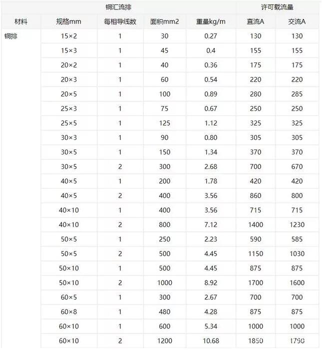
The usual PCB design current will not exceed 10 A, or even 5 A. Especially in household and consumer electronics, usually the continuous operating current on the PCB does not exceed 2 A. However, recently we have to design power wiring for the company's products, and the continuous current can reach about 80 A. Considering the instantaneous current and leaving a margin for the entire system, the continuous current of the power wiring should be able to withstand more than 100 A.
Then the problem comes,What kind of PCB can withstand 100 A current?
EMC message:With the development of the times, more and more electronic and electrical equipment or system products need to be inspected and tested.Among them, EMC testing is one of the necessary inspection and testing indicators. However, EMC testing projects are relatively expensive, EMC laboratories are expensive to build, and most measurement equipment requires imported equipment. As a result, few inspection and testing institutions have the ability to build EMC laboratories. The EMC performance of the product is given during the design stage. If EMC factors are not considered during the design of general electronic products, it will easily lead to failure of the EMC test and fail to pass the testing or certification of relevant EMC regulations. For example, product design and R&D engineers design effective filter circuits according to needs and place them in the preamplifier of the product's I/O (input/output) interface, which can eliminate the interference noise that enters the system due to conduction at the entrance of the circuit system; design isolation circuits (such as transformer isolation and photoelectric isolation, etc.) Solve the conduction interference entering the circuit through power lines, signal lines and ground wires, while preventing interference caused by public impedance and long-term transmission; design energy absorption loops to reduce the noise energy absorbed by circuits and devices; reduce the impact of interference by selecting components and rationally arranging circuit systems.
Disclaimer: This article is reproduced from "Quality Improvement and Technology", which supports the protection of intellectual property rights. Please indicate the original source and author of the reprint. If there is any infringement, please contact us to delete it.
Related Recommendations
Exclusive Interview with Li Gang of Yunfan Ruida: The Precision of Millimeter-Wave Radar Products and the Warmth of Humanity
2026-07-22
2501
RF Passion, Craftsman’s Journey: Over 30 Years of Steadfast Dedication — Interview with Kinghelm Chief Engineer Mr. Qin hongxiang
2026-06-26
2675





 粤公网安备44030002007346号