
























Service Hotline
News

News
Do you know the meaning of each layer of PCB?
2022-03-16
821
PCB layer Chinese and English name
|
English |
Chinese |
|
|
mechanical |
mechanical layer |
|
|
keepout layer |
Disable routing layer |
|
|
top overlay |
Silk screen layer |
Top silk screen layer |
|
bottom overlay |
Bottom silk screen layer |
|
|
top paste |
Soldering flux (tinning) layer |
top pad layer |
|
bottom paste |
Bottom pad layer |
|
|
top solder |
solder mask |
Top solder mask |
|
bottom solder |
Bottom solder mask |
|
|
drill guide |
via layer |
via guide layer |
|
drill drawing |
via drilling layer |
|
|
multilayer |
multi-layer |
|
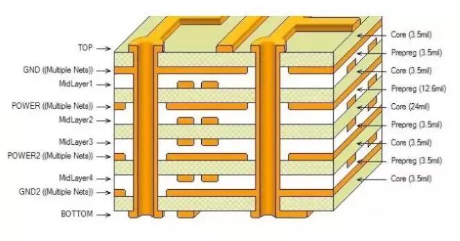
The mechanical layer defines the appearance of the entire PCB board. In fact, when we talk about the mechanical layer, it refers to the appearance structure of the entire PCB board.
The prohibited wiring layer defines the boundary when we lay out copper with electrical characteristics. That is to say, after we first define the prohibited wiring layer, in the subsequent laying process, the lines with electrical characteristics we lay cannot exceed the boundary of the prohibited wiring layer.
Top overlay and bottom overlay are the silk screen characters that define the top and bottom layers, which are generally the component numbers and some characters we see on the PCB board.
Top paste and bottom paste are the top and bottom pad layers, which refer to the exposed copper platinum that we can see. For example, if we draw a wire on the top wiring layer, what we see on the PCB is just a wire. It is covered by the entire green oil, but if we draw a square or a point on the top paste layer at the position of this wire, the square and point on the printed board will not have green oil, but copper platinum.
The two layers of top solder and bottom solder are just opposite to the previous two layers. It can be said that these two layers are the layers to be covered with green oil.
The multilayer layer is actually almost the same as the mechanical layer. As the name implies, this layer refers to all layers of the PCB board.
The pads and through-holes on the circuit board need to penetrate the entire circuit board and establish electrical connections with different conductive pattern layers. Therefore, the system specially sets up an abstract layer - multi-layer. Generally, the pads and vias are arranged on multiple layers. If this layer is closed, the pads and vias cannot be displayed.
The difference between solder mask and flux layer
Solder mask:The solder mask refers to the part of the board that needs to be coated with green oil; because it is a negative output, the actual effect of the part with the solder mask is not coated with green oil, but tinned, making it silvery white.
Soldering layer:Paste mask is used when machine mounting. It corresponds to the pads of all patch components. It is the same size as the top layer/bottom layer. It is used to open the steel mesh and leak tin.
Please note:
Both layers are used for tin soldering, which does not mean that one is tinned and the other is coated with green oil. So is there a layer that refers to the layer that is coated with green oil? As long as there is this layer on a certain area, it means that this area is coated with insulating green oil? I have not encountered such a layer yet.
The pads on the PCB we drew have a solder layer by default, so the soldering pads on the finished PCB are coated with silver-white solder and are not coated with green oil.
That can be understood like this:
1. The solder mask layer means opening a window on the entire solder mask green oil to allow welding.
2. By default, areas without solder mask are painted with green oil.
3. The paste mask layer is used for patch packaging.
SMT packaging is used:
top layer, top solder layer, top paste layer,
And the top layer and top paste are the same size,
The top solder is slightly larger than them.
DIP packaging only uses:
top solder and multi layer
(After some decomposition, I found that the multi layer layer is actually the top layer, bottom layer, top solder, and bottom solder layer with overlapping sizes),
And the top solder/bottom layer is larger than the top layer/bottom layer.
Question: "The copper layer corresponding to the solder layer will be tinned or gold-plated only if there is copper." Is this correct?
This sentence was said by a person who works in a PCB factory. What he means is: if you want the part painted on the solder layer to produce a tin-plated effect, then the corresponding solder layer part must have copper skin (that is: the area corresponding to the solder layer must have a top layer or bottom layer part).
Now, I have come to a conclusion: "The copper layer corresponding to the solder layer will be tinned or gold-plated only if there is copper." This sentence is correct. The solder layer represents the area not covered by green oil.
Disclaimer: This article is reproduced from "actSMTC", which supports the protection of intellectual property rights. Please indicate the original source and author of the reprint. If there is any infringement, please contact us to delete it.
Company phone number: +86-0755-83044319
Fax/FAX: +86-0755-83975897
Email: 1615456225@qq.com
QQ: 3518641314 Manager Li
QQ: 332496225 Manager Qiu
Address: Room 809, Building C, Zhantao Technology Building, No. 1079 Minzhi Avenue, Longhua New District, Shenzhen
Related Recommendations
Exclusive Interview with Li Gang of Yunfan Ruida: The Precision of Millimeter-Wave Radar Products and the Warmth of Humanity
2026-07-22
2501
RF Passion, Craftsman’s Journey: Over 30 Years of Steadfast Dedication — Interview with Kinghelm Chief Engineer Mr. Qin hongxiang
2026-06-26
2673





 粤公网安备44030002007346号