
























Service Hotline
News

News
IC packaging knowledge: wafer level packaging technology
2022-03-16
2004
Traditionally, the electrical connection between the IC chip and the outside is achieved by using metal wires to connect the I/O on the chip to the package carrier through bonding and through the package pins. As the feature size of IC chips shrinks and the integration scale expands, the spacing of I/Os continues to decrease and the number continues to increase. When the I/O spacing shrinks to less than 70 um, wire bonding technology is no longer applicable, and new technical approaches must be sought. Wafer-level packaging technology uses thin film redistribution processes so that I/O can be distributed on the entire surface of the IC chip instead of just being limited to the peripheral area of the narrow IC chip, thereby solving the electrical connection problem of high-density, fine-pitch I/O chips.
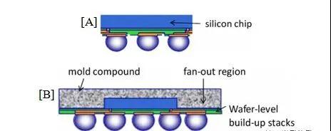
Among the many new packaging technologies, wafer-level packaging technology is the most innovative and attracts the most attention from the world. It is a symbol of revolutionary breakthroughs in packaging technology. Wafer-level packaging technology uses wafers as the processing object. Numerous chips are packaged, aged, tested, and finally cut into individual devices on the wafer. It reduces the package size to the size of an IC chip and significantly reduces production costs. The advantages of wafer-level packaging technology have caused it to receive great attention as soon as it appeared and quickly gained huge development and wide application. In portable products such as mobile phones, wafer-level packaged EPROM, IPD (integrated passive devices), analog chips and other devices have been widely used. The number of device categories using wafer-level packaging is increasing, and wafer-level packaging technology is a rapidly developing new technology.
In order to improve the applicability of wafer-level packaging and expand its application scope, people are researching and developing various new technologies while solving problems that arise during the industrialization process, and conducting research on the current status, application, and development of wafer-level packaging technology.
Wafer level packaging
The initial germination of WLP was driven by the manufacturing of low-speed I/O (low-I/O) and low-speed transistor components for mobile phones, such as passive on-chip sensors and power transmission ICs. Currently, WLP is in the development stage. Driven by applications such as Bluetooth, GPS (global positioning system) components, and sound cards, demand is gradually growing. When it reaches the 3G mobile phone production stage, it is expected that a variety of new mobile phone content applications will become another growth driver for WLP, including TV tuners, FM transmitters and stack memories. As storage device manufacturers begin to gradually implement WLP, it will lead to paradigm changes in the entire industry.
At present, wafer-level packaging technology has been widely used in fields such as flash memory, EEPROM, high-speed DRAM, SRAM, LCD drivers, radio frequency devices, logic devices, power/battery management devices and analog devices (voltage regulators, temperature sensors, controllers, operational amplifiers, power amplifiers). Wafer-level packaging mainly uses two basic technologies: film redistribution technology and bump formation. The former is used to convert the solder areas distributed along the periphery of the chip into bump solder areas distributed in a planar array on the chip surface. The latter is used to make bumps on the bump pad area to form a solder ball array.
Thin film redistribution WL-CSP
Membrane redistribution WL-CSP is the most commonly used process today. Because of its low cost, it is very suitable for the requirements of high-volume, portable product board-level application reliability standards. Like other WLPs, the wafers of thin-film redistribution WL-CSP are still manufactured using conventional wafer processes. Before the wafers are sent to the WLP supplier, the wafers are tested to classify the circuits and draw wafer diagrams of qualified circuits. Before redistributing wafers, the layout of the device must be evaluated to confirm whether the wafer is suitable for solder ball redistribution.
A typical redistribution process, the final solder bumps are in an area array layout. In this process, BCB is used as the redistribution dielectric layer, Cu is used as the redistribution connection metal, sputtering is used to deposit the bump bottom metal layer (UBM), and screen printing is used to deposit solder paste and reflow. The bottom metal layer process is very critical to reduce intermetallic chemical reactions and improve interconnection reliability.
The redistribution process is to rearrange the I/O pads on the device surface. Figure 3 shows the redistribution situation on the bonded flash memory. As can be seen from the figure, the original pads on the four sides of the flash memory chip are converted into an array of bumps. In this example, two dielectric layers are used on the device surface, with a redistribution metallization layer sandwiched in between to change the I/O distribution. After this process, solder ball bumps are electroplated, and the chip becomes a WLP product.
The disadvantage of redistributing the wire bond pad design into solder ball array pads is that the resulting WLP product is unlikely to be optimal in terms of device design, construction, or manufacturing cost. However, once it is proven technically feasible, the circuit can be redesigned so that external redistribution can be eliminated. This situation has become a consensus. For this purpose, a biphasic determination procedure is specially defined. Next-generation changes may be the integration of redistribution layers within the last metal layer of the chip, or a new design of the shortest signal lines to improve performance.
Sacco Micro SLKOR product linear voltage regulator chip SL78L05
Redesign may require the addition of new software tools. The redesigned signal, power, and ground lines are very inexpensive to construct since they eliminate additional redistribution steps and associated processes. Polymers are used for silicon wafer planarization, providing necessary chip protection, and as standard surface coatings. For thin-film redistribution WLP, the single-layer polymer WLP approach is a more cost-effective design.
Fabrication of wafer-level microbumps
Since its inception 50 years ago, wire bonding has been considered a versatile and reliable interconnect technology. However, with the rapid development of mobile communications, Internet e-commerce wireless access systems, Bluetooth systems and Umbrella Positioning System (GPS) technology, mobile phones have become the strongest and fastest growth driver of high-density memories. They are replacing PCs as the technology driver of high-density memories. The demand for lower cost, smaller form factor, higher speed device performance, longer battery life, better heat dissipation, "green" processes and higher device reliability has led designers to turn their attention to flip-chip bump interconnect technology to replace traditional wire bonding technology.
The key technical driving force for the development of lead-tin bump technology comes from the continued shrinking of device size. Under the 130nm technology standard, about 30% of logic chips require bump technology. However, under the 90 nm technology standard, this figure jumped to 60%. When the mass production of 65 nm devices was developed, the demand for gold bump technology climbed to more than 80%.
WLP is based on BGA technology and is an improved and enhanced CSP. Some people also call WLP wafer-level chip size packaging (WLP-CSP). It not only fully reflects the technical advantages of BGA and CSP, but also marks a revolutionary breakthrough in packaging technology. Wafer-level packaging technology adopts mass production process manufacturing technology, which can reduce the packaging size to the size of IC chips, significantly reduce production costs, and integrate packaging and chip manufacturing, which will completely change the separation of chip manufacturing and chip packaging industries. Precisely because wafer-level packaging technology is of such important significance, it has received great attention since its emergence and has rapidly gained tremendous development and wide application.
Under-bump metallization (UBM)
In flip-chip interconnection, the UBM layer is the critical interface layer between the metal pads and gold or solder bumps on the IC. This layer is one of the key elements of flip-chip packaging technology and provides high-reliability electrical and mechanical connections to both the circuitry and solder bump aspects of the chip. The UBM layer between the bumps and I/O pads needs to have good enough adhesion to the metal pads and wafer passivation layers; protect the metal pads during subsequent process steps; maintain low contact resistance between the metal pads and bumps; serve as an effective diffusion barrier between the metal pads and bumps; and serve as a seed layer for solder bump or gold bump deposition.
The UBM layer is usually achieved by depositing multiple layers of metal on the entire wafer surface. Techniques used to deposit UBM layers include evaporation, electroless plating and sputter deposition. In advanced packaging, wafer bumping is critical both from a cost and technology perspective. In wafer bump production, metal deposition accounts for more than 50% of the total cost. The most common metal deposition steps in wafer bump production are the deposition of under-bump metallization (UBM) and the deposition of the bumps themselves, which are generally achieved through an electroplating process.
Electroplating technology can achieve very narrow bump pitches and maintain high yields. Moreover, this technology has a wide range of applications and can produce bumps of different sizes, pitches and geometric shapes. Electroplating technology has been increasingly used in wafer bump production and has become the most practical solution.
First, the UBM layer is completed on the wafer. Thick glue is then deposited and exposed to light, forming a template for electroplating solder. After plating, the photoresist is removed and the exposed UBM layer is etched away. The last process is reflow to form solder balls. The detailed process steps for electroplating to produce microbumps are:
▲Evaporate/sputter the metal layer of the seed conductive layer on the wafer;
▲ Spin-coat a layer of photoresist on the wafer;
▲Photolithography electrode window array pattern;
▲Plating metal micro-embedded body through small holes in the photoresist;
▲Remove photoresist;
▲Etch the exposed conductive layer of the seed crystal.
▲Coat a thick layer of photoresist on the metal inlay;
▲Engrave Au bumps;
▲Etch away part of the thick glue to reveal the protruding part of the metal inlay;
▲Electroplating Au bumps;
▲Deposit a very thin layer of Au or Cu on top of the inlay.
Coplanarity refers to the consistency of the heights of all bumps within the wafer, which has strict requirements in the flip-chip bonding process. In flip-chip bonding, bump height variations can lead to uneven distribution of force, chip fragmentation, and electrical opens. A typical requirement for bump coplanarity is that the height difference of the bumps across the entire chip cannot be greater than 5 μm.
thick film lithography
Wafer-level process technologies such as fine-pitch wafer bumping, lead pad redistribution and integrated passive components provide convenient solutions for many applications. Currently, many IC and MEMS devices have applied these technologies. Using these technologies, devices can be packaged and tested at the wafer level, followed by subsequent dicing processes. Usually advanced packaging technology involves thick film processes of 5 to 100 μm, such as thick glue spin coating, uniform exposure of thick glue with large undulations on the surface, and obtaining very steep thick glue sidewalls. The equal-magnification full-field exposure system is an equipment solution that can meet this demand. Its high output and low self-alignment cost make it the most competitive system for projection steppers in the field of thick film lithography.
Wafer-level packaging processes include metallization, photolithography, dielectric deposition and thick film photoresist spin coating, solder deposition and reflow soldering. The patterning process typically involves using several layers of metal to create the under-bump metallization (UBM) layer that serves as the base for the bumps. The conductivity of the connection between the bumps and the wafer must be very good, and the passivation layer and the metal layer under the bumps must have good adhesion. The standard process flow of photoresist patterning includes cleaning, glue coating, pre-baking, exposure, post-baking, development and film hardening. Each process step needs to define a set of parameters, which will affect subsequent processes. After the photoresist is patterned, the holes are filled with solder or gold through electroplating or evaporation. The next step is to remove the photoresist and perform a reflow process in an oven to convert the columnar bumps into spherical bumps.
Sacco Micro SLKOR products PNP transistors
A thick coating of photoresist will remain on the chip as a mask for making micro-molds of metal solder joints. The redistribution coating can be retrofitted into a bump pattern or as a connection between perimeter pads and area-distributed pad arrays made from 5 to 100 μm thick polysilicon films with varying electrical, chemical, mechanical and thermal properties. Isolating the redistribution area traces requires materials with high strength, high thermal stability, and low insulation coefficients. These materials have been successfully developed. One type of material is called polyimide (such as the PI series developed by DuPont), and the other insulating material is Cyclotene (BCB) from Dow Chemicals in the United States. PI and BCB are widely used in flip chip bump packaging and other packaging processes.
Micro-featured molds using thick-film photoresist pads, bumps, and under-ball metal layer structures can meet different needs in WLP. Although commonly used metallization materials are tin-lead, gold, and copper, several other materials can also be used. Materials used in standardized applications require high-resolution graphic transfer and easy peel-off properties. Many practical applications require photoresist thicknesses exceeding 100μm. To achieve such thicknesses, manufacturers develop suitable coating materials.
In order to meet these needs, manufacturers have developed corresponding materials and process equipment. Many materials can achieve "thin" photoresist coatings (i.e. 2-10 μm) on standard semiconductor process equipment. AZP4330 (Anzhi Electronic Materials Group) and Shipley's 955 (Rohm & Haas Company/Shipley Company) photoresists are used to achieve a photoresist film thickness of 5 to 100 μm. A photoresist coating with a film thickness of 25 μm can be achieved using a multi-layer coating process, but this will increase production time and cost. AZ P4620 and SPR 220 can achieve a thickness of 25 μm in a single layer. For thicker coatings, the choice of materials and thicknesses becomes smaller. There are many cost benefits when using a single layer deposition to achieve the desired photoresist coating. Therefore, it is very necessary to develop photoresist materials with a single layer thickness of 50 μm and above. Materials such as JSR THB-611P and Anzhi Electronic Materials Group's AZPLP100XT can achieve a single layer of photoresist coating with a thickness of 60 μm and above. Recent research work mainly uses AZ9260 to realize a single layer of 65 μm thick photoresist coating and uses AZ50XT to realize a single layer of 100 μm thick photoresist.
The thick film process has some special requirements for the system. The alignment system must be able to uniformly identify the geometric pattern as the alignment mark over the entire range of glue thickness and specific heights of wafer surface relief. Since the exposure source uses parallel light for exposure without relying on focus, it can be achieved by using a proximity lithography machine combined with the principle of shadow exposure. The requirements of the photolithography process for proximity mask alignment exposure machines include: high intensity, high uniformity, UV light wavelength consistent with the sensitive wavelength of the photoresist, sub-micron alignment accuracy, and an accurate, controllable and consistent gap between the mask and the wafer during the exposure process.
EVG's NanoAlign technology is designed with the highest alignment accuracy and resolution and the lowest cost of use to highlight the advantages of full-field exposure technology. Currently, all of his company's exposure machines have applied this technology. Its goals include active anomaly control and sub-100 nm dynamic alignment resolution. Its equipment includes specialized glue coating equipment and contact/proximity exposure machines modified from standard models. The latest 200 mm EVG6200 Infinity and 300 mm EVG IQ Aligner exposure machines have good flexibility and user-friendly interface, and can fully meet the industrial production of φ200 mm and φ300 mm wafers that require thick glue processes.
Wafer thinning
Chip thinning technology is crucial in stacked chip packaging technology because it reduces the package mounting height and allows chips to be stacked without increasing the overall height of the stacked chip system. Smart cards and RFID are the thinnest single-chip applications that are an important part of the thin wafer requirements. Thinner chips increase thermal cycle reliability and support thin products. However, how thin the chip is depends on the wafer diameter and the WLP process. The reason is that the thin wafer surface is prone to damage, causing micro-cracks, and causing the wafer to break during subsequent operations. Since wafer backside grinding is the final step of the wafer processing process, the extent to which the wafer needs to be thinned is limited by the WLP process. Therefore, wafer-level packaging is regarded as an extension of the wafer process, and the applicable scope of the packaging process steps should be taken into consideration when designing the wafer process.
Poor matching of thermal expansion coefficients between silicon and mounting substrate is an important reason for fatigue failure of packaged solder balls in thermal cycle tests and field use. In addition, this failure is also closely related to how strong each component is. The thinner the chip, the more flexible it will be, and the fatigue resistance of the solder ball will be improved. Therefore, thinning the wafer and thus reducing the chip thickness is also one of the important measures to improve the reliability of solder bumps. Thinning the wafer before wafer-level packaging processing can easily deform or even break the wafer, which is undesirable. Wafer thinning after wafer-level packaging processing is completed is a better method, but it is difficult to implement. Wafer and thinning technologies and equipment for wafer-level packaging manufacturing are under development.
Advantages of wafer-level packaging
Wafer-level packaging is based on BGA technology and is an improved and improved CSP, which fully reflects the technical advantages of BGA and CSP. It has many unique advantages:
① The packaging processing efficiency is high, and it is manufactured using a mass production process in the form of wafers;
② It has the advantages of flip-chip packaging, that is, light, thin, short, and small;
③The cost of wafer-level packaging production facilities is low, and wafer-level manufacturing equipment can be fully utilized without the need to invest in building another packaging production line;
④The chip design and package design of wafer-level packaging can be considered uniformly and carried out simultaneously, which will improve design efficiency and reduce design costs;
⑤ In the entire process of wafer-level packaging from chip manufacturing, packaging to product shipment to users, the intermediate links are greatly reduced and the cycle is shortened a lot, which will inevitably lead to cost reduction;
⑥The cost of wafer-level packaging is closely related to the number of chips on each wafer. The more chips there are on a wafer, the lower the cost of wafer-level packaging. Wafer level packaging is the smallest low-cost package. Wafer-level packaging technology is a true mass production chip packaging technology.
The advantage of WLP is that it is a chip-scale packaging (CSP) technology suitable for smaller integrated circuits. Due to the use of parallel packaging and electronic test technology at the wafer level, it can significantly reduce the chip area while increasing output. Since parallel operations are used for chip connections at the wafer level, the cost of each I/O can be greatly reduced. In addition, adopting simplified wafer-level test procedures will further reduce costs. Wafer-level packaging can be used to package and test chips at the wafer level.
Development trends of wafer-level packaging technology
Wafer-level packaging technology must strive to reduce costs, continuously improve reliability levels, and expand its application in large ICs. In terms of solder ball technology, Pb-free solder ball technology and high-Pb solder ball technology will be developed. With the continuous expansion of IC wafer size and the advancement of process technology, IC manufacturers will research and develop a new generation of wafer-level packaging technology. This generation of technology can not only meet the needs of φ300 mm wafers, but also adapt to the recent requirements of copper wiring technology and low dielectric constant interlayer dielectric technology. In addition, there is also a requirement to improve the ability of wafer-level packaging to handle current and withstand temperature. WLBI (wafer level testing and aging) technology is also an important topic that needs to be studied. WLBI technology is to conduct electrical testing and aging directly on IC wafers, which is of great significance to simplifying the process flow and reducing production costs for wafer-level packaging.
Sacco Micro SLKOR Products Schottky Diodes
Conclusion
Wafer-level packaging technology is a low-cost mass production chip packaging technology. Wafer-level packaging is the same size as a chip and is the smallest micro surface mount device. Due to a series of advantages of wafer-level packaging, wafer-level packaging technology is developing vigorously driven by the demand for miniaturization and low-cost of modern electronic devices. Currently, wafer-level packaging technology is usually suitable for small-size chips with low I/O numbers. The industry also needs to develop new technologies to reduce production costs and develop wafer-level packaging of large-size chips and fine-pitch solder ball array wafer-level packaging.
When selecting a package type for modern electronic devices, it is important to meet design requirements while minimizing cost. The current level of wafer-level packaging is only an alternative packaging type. There is still a lot of work to be done to make wafer-level packaging technology a mainstream manufacturing technology for large-volume and wide-ranging products in the future. Combining the design of semiconductor chips and WLP packages will undoubtedly bring benefits to the layout of WLP devices and improve device performance. In WLP, since the packaging steps of all devices on the wafer are performed simultaneously, batch processing can reduce packaging costs. (This article is excerpted from "Special Equipment for the Electronic Industry")
Attachment: The difference between Fan-in and Fan-out
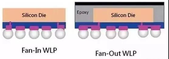
From the perspective of technical characteristics, wafer-level packaging is mainly divided into two types: Fan-in and Fan-out. Traditional WLP packaging mostly adopts Fan-in type and is used in ICs with low pin count. However, as the number of IC signal output pins increases, the requirements for the ball pitch (Ball Pitch) become more stringent. In addition, the printed circuit board (PCB) construction requires adjustment of the post-IC packaging size and the position of the signal output pins. Therefore, various new WLP packaging types such as diffused (Fan-out) and Fan-in plus Fan-out have been derived. The manufacturing process even breaks away from the traditional WLP packaging concept.
According to Zhou Xiaoyang, President of Amkor China: The chip size using Fan-in packaging is the same as the product size on the two-dimensional plane, and the chip has enough area to put all the I/O interfaces. When the size of the chip is not enough to accommodate all I/O interfaces, Fan-out is required. Of course, the general Fan-out also adds active and/or passive components to form a SIP while expanding the area.
Let’s talk about the fan-in type first.
According to a report from Mammes Consulting. Fan-in packaging technology has been successfully applied and has grown steadily for more than ten years. It remains attractive today due to its inherent, unparalleled combination of smallest package size and low cost. With these advantages, it has gradually penetrated into the size-driven handheld device and tablet market and still maintains strong vitality in these device fields. It is estimated that more than 90% of fan-in packaging technology is currently used in the mobile phone field. Talking about the application of fan-in packaging technology, more than 30% of all packaged devices in high-end smartphones now use fan-in packaging. Therefore, fan-in packaging technology is still in its golden period of business in the mobile phone field.
Although the growth pace of fan-in packaging technology has been stable so far, changes in the global semiconductor market and the growth of uncertainties in future applications will inevitably affect the future prospects of fan-in packaging technology. As smartphone shipment growth dropped from 35% in 2013 to 8% in 2016, and this number is expected to further decline to 6% by 2020, the application of fan-in packaging technology led by the smartphone market is becoming increasingly saturated. Although the expected high growth is not optimistic, smartphones are still the main driving force for the development of the semiconductor industry, and smartphone shipments are expected to reach 2 billion units in 2020.
Currently, the main fan-in packaged devices are WiFi/BT (wireless LAN, Bluetooth) integrated components, transceivers, PMIC (power management integrated circuits) and DC/DC converters (accounting for about 50% of the total), as well as various digital, analog, and mixed-signal devices including MEMS and image sensors. The biggest challenge that fan-in packaging technology may face in the future may be the integration of device functions in system-level packaging. The figure below shows the impact of the growth of system-level packaging on fan-in packaging shipments. Its overall compound annual growth rate dropped from 9% to 6%. This report provides a detailed analysis of the growth of system-in-package and its impact on fan-in packaging.
As for the fan-in market, statistics from 2015 show that outsourced semiconductor packaging and testing occupies a major market share, including an IDM manufacturer (TI, Texas Instruments) and a foundry (TSMC, TSMC). STATS ChipPAC has shown strong leapfrog development after being acquired by JCET. On the design side, Qualcomm and Broadcom drive 50% of the entire fan-in packaging market.
Regarding packaging technology, in the past few years, the market has mostly focused on the development of fan-out wafer-level packaging technology. However, fan-in packaging has carved out its own development path and roadmap. In addition to further expansion, it can still bring other types of innovative technologies, such as six-sided mold protection. This report provides a detailed analysis of two fan-in packaging technology roadmaps: one for high volume volume manufacturing (HVM) and the other for production readiness. The path map includes I/O counters, L/S, bump pitch, package thickness, dimensions, etc. In addition, this report also analyzes fan-in packaging technology from the perspective of utilizing IC technology nodes and further front-end expansion of fan-in IC devices. Although the HVM production path of fan-in packaging technology expands slower than that of fan-out packaging technology, fan-in packaging technology has the ability to meet the expansion conditions of most fan-out packaging and has a production-ready development path that is readily available.
Next, let’s talk about the fan-out type.
Fan-out packaging adopts the method of pulling out wires, which is relatively cheap; fan-out WLP allows a variety of different die to be buried like the WLP process, which is equivalent to reducing one layer of packaging. If multiple die are placed, it is equivalent to eliminating multi-layer packaging, which helps reduce customer costs. The only factor that affects IC cost at this time is die size.
Since 2013, major packaging and testing factories around the world have been actively expanding FOWLP production capacity, mainly to meet the stringent cost requirements of the mid- to low-price smartphone market. Because FOWLP does not require the use of carrier board materials, it can save nearly 30% of packaging costs, and the packaging thickness is also thinner, helping to improve the competitiveness of chip manufacturers' products.
A report from Memes Consulting shows that 2016 is a turning point in the fan-out packaging market. The addition of Apple and TSMC has changed the application status of this technology and may make the market gradually begin to accept fan-out packaging technology. The fan-out packaging market will be divided into two types:
- The "core" market for fan-out packaging, including single-chip applications such as baseband, power management, and RF transceivers. This market is the main application area for fan-out wafer-level packaging solutions and will maintain a stable growth trend.
- The "high-density" market for fan-out packaging started with Apple's APE, including processors, memories and other applications with larger input and output data volumes. This market has greater uncertainty and requires new integrated solutions and high-performance fan-out packaging solutions. However, this market has great market potential.
As fan-out packaging technology has a huge potential for "high-density" markets and "core" markets with stable growth, the supply chain in this area is expected to invest heavily in fan-out packaging capabilities. Some manufacturers are already able to offer fan-out wafer-level packaging, but many others are still in the development stage of fan-out packaging platforms in order to enter the fan-out packaging market and expand their product portfolios.
In addition to TSMC, STATS ChipPAC (Singapore STATS ChipPAC) will use the support of JCET (Jiangsu Changdian Technology) to further invest in the development of fan-out packaging technology (in early 2015, Jiangsu Changdian Technology acquired Singapore STATS ChipPAC for US$780 million); ASE (ASE Group) has established an in-depth cooperative relationship with Deca Technologies (In May 2016, Deca Technologies Technologies received a US$60 million investment from ASE Group, and ASE Group obtained Deca Technologies' M series fan-out wafer-level packaging technology and process authorization); Amkor (Ankor Technology), SPIL (Silicon Products Technology) and Powertech (Powertech) are aiming at future mass production and are in the development stage of fan-out packaging technology. Samsung appears to be lagging behind as it decides how to compete.
In terms of market capacity, fan-out packaging maintains a compound annual growth rate of 56%, which will bring broad prospects to packaging and testing manufacturers in the future.
But this new technology will still face great challenges in the future. Zhou Xiaoyang, president of Amkor China, said that Fan-out technology will have great demand in application fields that are smaller, thinner and faster. The current cost of Fan-out is relatively high and requires further technical optimization. In addition to wafer-based technology, many manufacturers are also doing panel-based technology.
Currently, TSMC is also one of the main promoters of Fan-out technology, while Amkor and other major packaging and testing companies also have different forms of unique Fan-out technologies. Relatively speaking, the current Fan-out technology is not very mature, and its yield and reliability need to be further improved.
Note: This article is reproduced from the Internet and supports the protection of intellectual property rights. Please indicate the original source and author when reprinting. If there is any infringement, please contact us to delete it.
Company phone number: +86-0755-83044319
Fax/FAX: +86-0755-83975897
Email: 1615456225@qq.com
QQ: 3518641314 Manager Li
QQ: 332496225 Manager Qiu
Address: Room 809, Building C, Zhantao Technology Building, No. 1079 Minzhi Avenue, Longhua New District, Shenzhen
Related Recommendations
Exclusive Interview with Li Gang of Yunfan Ruida: The Precision of Millimeter-Wave Radar Products and the Warmth of Humanity
2026-07-22
3238
RF Passion, Craftsman’s Journey: Over 30 Years of Steadfast Dedication — Interview with Kinghelm Chief Engineer Mr. Qin hongxiang
2026-06-26
3302





 粤公网安备44030002007346号