
























Service Hotline
News

News
International Semiconductor Equipment Company Ranking
2022-03-16
1825
International Semiconductor Equipment Company Ranking
??The latest ranking of global and domestic semiconductor equipment factories! Japanese manufacturers are leading the way, while mainland Chinese manufacturers have accumulated a lot of experience.
??1. US Applied Materials (Applied Materials)
??U.S.-based Applied Materials has held the top spot since 2007, and has maintained its leadership position except in 2011 when it was taken over by ASML, the world's largest semiconductor lithography equipment manufacturer. Applied Materials is a leader in materials engineering solutions used to produce nearly all of the world’s new chips and advanced displays. Applied Materials' sales in 2019 reached US$13.4 billion, down 3.9%.
??2. Dutch ASML (ASML)
??ASML has gradually approached the market size of Applied Materials. According to ASML financial report data, ASML's net sales in 2019 were 11.8 billion euros and net income was 2.6 billion euros. According to Statista Research, as of 2019, most of ASML's sales revenue came from Asia, which was 9.5 billion euros, while the company's sales revenue in the United States and Europe, the Middle East and Africa were 2 billion euros and 300 million euros respectively. ASML's total net revenue has grown every year from 2014 to 2019. In 2014, the Dutch multinational company achieved net revenue of approximately 5.9 billion euros. In 2019, this number doubled, and ASML generated approximately 11.8 billion euros in revenue.
??For ASML, 2019 was another growth year, mainly due to strong demand for DUV and EUV logic, with its EUV order book of 6.2 billion euros and witnessing the adoption of EUV in high-volume production.
??3. Tokyo Electron, Japan
??Tokyo Electronics’ 2019 ranking is consistent with that of 2018, still ranked third. Sales in 2019 were US$9.55 billion, a year-on-year decrease of 12.5%. TEPCO's products cover almost all processes in the semiconductor manufacturing process. Its main products include: glue coating/developing equipment, heat treatment film forming equipment, dry etching equipment, deposition equipment, cleaning equipment, and packaging and testing equipment. Among them, glue coating/developing equipment accounts for 87% of the world's share, and among FPD manufacturing equipment, etching machines account for 70%.
??4. Lam Research (USA)
??The sales volume of LAM in 2019 was close to that of Tokyo Electronics, which ranked third, both at around US$95, down 12.2%. For semiconductor companies, fourth-ranked LAM Research is a fundamental driver of the silicon technology roadmap, with the company focusing on the etching, deposition and cleaning markets. Over the past few years, Lam Research has grown its share of the etch and deposition space, thanks to the increasing layer count of 3D NAND and the foundry/logic transition to the 10/7nm process node, which requires more multiple patterning steps. These vertical scaling-related technologies rely heavily on advanced etch and deposition tools. It is reported that 80% of Lam's revenue is related to memory chips (solid-state flash memory and DRAM). LAM's flagship Kiyo, Vector and Saber products are mainly sold to major customers such as Samsung Electronics and TSMC.
??5. KLA-Tencor of the United States
??KLA, ranked fifth, had sales of US$4.66 billion in 2019, an increase of 10% compared to last year. Compared with the first tier, KLA's sales were about half of the top four. However, in today's semiconductor testing equipment market, KLA is the absolute king in the world. According to SEMI statistics, KLA accounted for more than half of the front-end inspection and measurement market in 2018, ranking first in the industry, and can be called the king in the field of semiconductor inspection equipment. KLA has long dominated the market for equipment that inspects semiconductor photomasks and reticles. Customers in international markets account for more than 75% of the company's revenue. In February 2019, KLA acquired Israeli company Orbotech for approximately $3.2 billion. With this acquisition, KLA diversifies its revenue base and adds $2.5 billion in addressable market opportunities in PCB, FPD, packaging and semiconductor manufacturing.
??6. Japan Advantest (Advantest)
??Japan’s Advantest ranked sixth, with sales of US$2.47 billion in 2019, a 4% decline. In 1972, Advant officially entered the field of semiconductor testing. After more than 40 years of development, the company has become a global leader in back-end testing equipment. In the memory test bench market segment, Advant has long ranked first in the world with a market share of 40%. Advantest's main products include automated test equipment, SoC test systems, memory test systems, mechatronics test systems, etc. Advantest has developed many of Japan's "first" test equipment, creating a precedent in the Japanese testing industry.
??7. Japan Screen Semiconductor Solutions
??SCREEN, which has a high proportion of global semiconductor cleaning equipment, still maintains the same ranking as in 2018, ranking seventh. SCREEN's sales were close to those of Advantest, at $2.2 billion, down 1.2% from last year. Japan's SCREEN is the world's only comprehensive manufacturer of production line image plate making equipment and electronic original manufacturing equipment. It was founded in 1943. As early as 2008, SCREEN occupied the largest global share of the LCD manufacturing equipment market for coaters/developers, wet etching machines and resist strippers. In 2009, SCREEN gained more than 60% of the global share in single wafer cleaning systems.
??8. American Teradyne
??Teradyne, ranked eighth, is the only equipment provider that can cover analog, mixed-signal, memory and VLSI device testing. Teradyne's sales in 2019 increased 4.1% from the previous year to $1.55 billion. In 2019, the company's test bench market share ranked first in the world, and it was the absolute leader in SoC test benches. Teradyne automates two of the most critical elements in manufacturing: repetitive manual tasks and electronic testing. Teradyne's automated test equipment (ATE) accelerates time to market for new electronic products in markets where reliability and performance are critical.
??9. Japan’s Hitachi High-Technologies (Hitachi High-Technologies)
??Hitachi High-tech, which has an advantage in SEM length measurement equipment, has been promoted to TOP9. The sales of Hitachi High-Tech and Teradyne are also very close, at US$1.53 billion, a year-on-year increase of 9.3%. The semiconductor manufacturing equipment provided by Hitachi High-Tech mainly includes dry etching systems, CD-SEM and defect inspection. Hitachi High Technologies generates 42% of its sales from Japan. Hitachi owns nearly 52% of the company.
??10. ASM International of the Netherlands (Xianyu)
??ASM international (ASMi) also improved from 13th in 2018 to 10th. Its sales in 2019 were US$1.26 billion, making it one of the top fifteen companies with greater growth, an increase of 27.2% over last year. ASMi is a leading supplier of semiconductor processing equipment for wafer processing. It is a global company located in 14 countries. ASMi has pioneered the industrial use of many proven wafer processing technologies, including photolithography, deposition, ion implantation and single-wafer epitaxy. In recent years, ASMi has brought atomic layer deposition (ALD) and plasma-enhanced atomic layer deposition (PEALD) from R&D to mainstream production at advanced manufacturer sites.
??11. Japan Nikon (Nikon)
??The most eye-catching one is Nikon. In 2018, Nikon, which was engaged in exposure equipment, was still outside the TOP15, but in 2019, it jumped to the TOP11. Among the TOP15, Nikon made the greatest progress! In 2019, Nikon's sales reached US$1.2 billion, which doubled compared to 2018, reaching a growth rate of 117.8%. Nikon was founded in 1917. It first made its fortune through cameras and optical technology. It launched the first FPD exposure equipment in 1986 and now has a wide range of business lines.
??12. Japan Kokusai Electric (International Electric)
??In addition, the sales performance of Kokusai Electric, which specializes in heat treatment and other equipment, fell by 23.5%, and its ranking fell from ninth place in 2018 to 12th. In July 2019, Bloomberg reported that Applied Materials agreed to acquire Kokusai Electric from KKR & Co for approximately 250 billion yen ($2.2 billion). Kokusai Electric will operate as a business unit of Applied's Semiconductor Products Division and will continue to be headquartered in Tokyo. Kokusai specializes in batch processing, or processing many wafers in parallel, especially for storage wafers. According to reports, its main customers include Samsung Electronics Company, Taiwan Semiconductor Manufacturing Company and Intel Corporation.
??KOKUSAI ELECTRIC was originally Hitachi International Electric, and jointly competed with Hitachi High Technology in semiconductor equipment under the Hitachi Group. However, as Hitachi Manufacturing concentrated and screened its business, it was sold as a non-core business to Kohlberg Kravis Roberts (KKR), a U.S. private equity fund (Private Equity Fund) in 2017, and officially separated from the Hitachi Group. In addition, KKR consolidated the assets originally responsible for semiconductor production equipment and film forming process technology in Hitachi International Electric Group, and established a new organization-KOKUSAI ELECTRIC in June 2018. According to a report by the British Financial Times (Chinese name "Financial Times") on February 3, 2019, KKR is discussing selling part of KOKUSAI ELECTRIC's semiconductor equipment business (or all of its business) to a fund organization jointly owned by large Chinese companies and the Chinese government in order to obtain benefits. However, due to opposition from the U.S. and Japanese governments, industry insiders revealed that the sale should not be successful.
??13. Japanese Daifuku (large)
??Daifuku, which is engaged in semiconductor handling systems, grew by 13.9% compared to 2018, rising one place to 13th. The sales of Daifuku and Kokusai Electric are also relatively close, both at around US$1.1 billion. Daifuku's clean room storage and handling systems are widely used in semiconductor, LCD and other flat panel display manufacturing industries, and are sold by many world-renowned companies. Daifuku previously released financial data for the three quarters of 2019. Its orders, sales and operating income were mainly due to its reduced investment in the semiconductor and flat panel display sectors.
??14. Singapore ASM Pacific Technology
??ASM is part of the ASM International NV group, which also includes ASM Pacific Technology (ASMPT). ASMPT had the largest decline among the 15 companies, with sales falling 24.3% in 2019 to $890 million. It dropped from 11th last year to 14th. ASMPT was founded in 1975 and is headquartered in Singapore. It has been listed on the Hong Kong Stock Exchange since 1989. For this reason, VLSI regards it as a Chinese equipment manufacturer. ASMPT is a leading supplier of semiconductor process equipment for wafer assembly and packaging and surface mount technology and is the only company in the world to provide high-quality equipment for all major steps in the electronics manufacturing process, from carriers for chip interconnection to chip assembly and packaging to SMT.
??15. Japan Canon (Canon)
??In the field of FPD exposure equipment, two Japanese manufacturers, Nikon and Canon, occupy a major position, and they are also constantly competing for the FPD equipment market. It is understood that Canon is strong in the production of exposure equipment for large panels for TV displays, while Nikon's exposure equipment has more advantages in small and medium-sized panels for smartphone displays. Canon's sales ranking of semiconductor equipment manufacturers in 2019 is the same as last year, ranking 15th. However, its sales are far lower than Nikon, only US$690 million, down 9.5% from last year.
??Main problems faced by my country’s semiconductor equipment industry
??1. R&D investment is limited, and the technological gap is slow to catch up.
??Although my country's semiconductor equipment has made great progress in recent years and has achieved 0 breakthroughs in various fields, the overall R&D investment is still relatively low compared to overseas. In addition, the continuous advancement of advanced process nodes has made the domestic technology catch-up difficult. Although companies continue to increase their research and development efforts, with the evolution of Moore's Law, the more advanced the process, the higher the research and development costs. There are fewer and fewer semiconductor equipment manufacturers that can invest funds to keep up, which invisibly increases the difficulty of technological catch-up.
??Solution: Overcoming technical difficulties can be accomplished through the promotion of major national special projects. Enterprises and the government jointly undertake the technical overcoming of high-end equipment, reducing the pressure on R&D investment on the enterprise side. At the same time, we continue to encourage new domestic wafer fabs to promote local substitution of equipment, giving domestic semiconductor equipment manufacturers the opportunity to trial and error and improve. Formulate localization replacement node times for different semiconductor equipment, subsidize corporate R&D investment, and actively use various domestic financing channels to expand scale.
??2. Insufficient introduction of high-end talents, loss of core talents, and insufficient reserve talents
??Talent has become the bottleneck for the growth of China's semiconductor equipment industry. The cultivation of semiconductor talents is a long process, especially in terms of advanced processes and advanced technologies, and even spending money may not achieve the results. Salaries for industry talents are lower than overseas. Ensuring new talent is the key to continuing strong growth and breaking the growth bottleneck of the semiconductor equipment industry. In 2018, the number of graduates with bachelor's, master's and doctoral degrees nationwide exceeded 8 million, but only 30,000 college graduates in the field of integrated circuits entered the industry for employment.
??Actively introduce high-end talents through talent introduction, equity incentives, government subsidies, etc. The government takes the lead in promoting talent training in the semiconductor industry, through the integration of industry, academia and research, and at the same time provides policy preferences on issues such as housing for semiconductor industry talents.
3. Scientific layout, government guidance and reasonable planning. The early stage of the development of the integrated circuit industry must be led by the government. Currently, the investment entities in the integrated circuit industry are scattered, and the management entities are also very dispersed, which is very detrimental to the development of the industry. At this stage, it may be very important to formulate plans, establish strategies, scientific layout, and formulate policies. The government must manage, but cannot overmanage. If management is excessive, control will be blocked, regulations will increase, and policies will be multi-faceted, which may lead to low efficiency.
??5. Current status, problems and countermeasures of semiconductor materials
??The semiconductor materials industry is widely distributed and has many categories, including silicon and silicon substrates for wafer manufacturing, photoresists, high-purity chemical reagents, electron gases, targets, polishing fluids, etc. Classified by the upstream and downstream of the semiconductor industry chain, semiconductor materials can be divided into wafer manufacturing materials and packaging materials. The global wafer manufacturing materials and packaging materials markets in 2016 were US$24.7 billion and US$19.6 billion respectively. my country is the world's largest consumer of semiconductors and the world's largest demander of semiconductor materials. The global semiconductor materials market in 2016 was US$44.3 billion, of which mainland China's market sales were US$6.5 billion, accounting for 15% of the global total, surpassing semiconductor powers such as Japan and the United States, and ranking third in the world after Taiwan and South Korea.
??Like semiconductor equipment and other supporting facilities, my country's semiconductor materials also face problems such as insufficient self-sufficiency, small scale, and low proportion of high-end products. Compared with foreign companies, my country's semiconductor material companies are weak. However, with the support of national policies and the increase in R&D and industrial investment by domestic companies, breakthroughs have been made in various materials fields, and some domestic substitutions are gradually being realized.
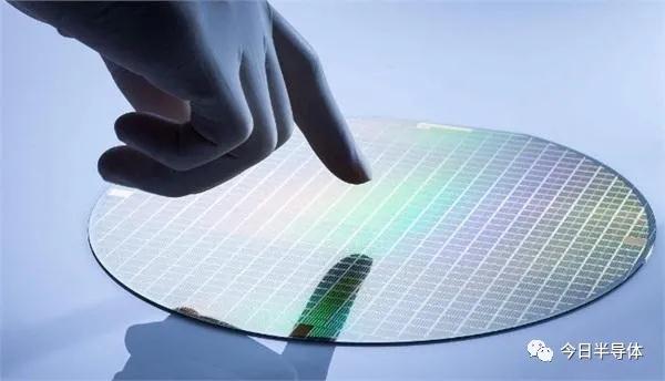
Below we focus on analyzing the current status, problems faced and countermeasures of several core semiconductor raw materials.
??1. Silicon wafer:
??Silicon single wafer is the most commonly used semiconductor material, which is essential in the chip production process and accounts for the highest cost. To manufacture a chip, ordinary silicon raw materials need to be first made into silicon single wafers, and then the silicon single wafers are made into chips through a series of process steps. In terms of market size, the global semiconductor silicon wafer market size was US$8.5 billion in 2016, accounting for 33% of the total scale of semiconductor manufacturing materials; the domestic semiconductor silicon wafer market size was RMB 11.9 billion in 2016, accounting for 36% of the total scale of domestic semiconductor manufacturing materials. Whether in the global or domestic market, silicon wafers account for the largest proportion of upstream materials in semiconductor manufacturing.
??The world’s five largest manufacturers (mainly German and Japanese manufacturers) account for almost 95% of the world’s 300mm silicon wafers, 86% of the world’s 200mm silicon wafers, and 56% of the world’s silicon wafers of 150 mm and below. This field is mainly monopolized by Japanese manufacturers. my country's localization rate of 6-inch silicon wafers is 50%, and the localization rate of 8-inch silicon wafers is 10%. 12-inch silicon wafers have not yet been mass-produced and are completely dependent on imports. Among the world's integrated circuit silicon wafer companies in 2017, Japan's Shin-Etsu Chemical has a 28% share, Japan's SUMCO has a 25% share, Taiwan's Global Wafer has a 17% share, Germany's Siltronic has a 15% share, and South Korea's LG has a 9% share. These five companies together account for 94% of the global share.
??2. Photoresist:
??The market for semiconductor photoresist is large, and there is a strong demand for domestic substitution. The total demand for China's photoresist market in 2015 was 4,390 tons, 5.7 times that of 2007. Currently, semiconductor photoresist suppliers are concentrated in the United States, Japan, Europe, South Korea and other places. China's photoresist suppliers are mostly concentrated in low-end fields such as PCB photoresist and LCD photoresist. Currently, domestic manufacturers capable of producing semiconductor photoresist include Beijing Kehua Microelectronics and Suzhou Ruihong.
??3. Target material:
??High-purity sputtering targets mainly refer to metal or non-metallic targets with a purity of 99.9%-99.9999% (between 3N-6N). They are used in the physical vapor deposition (PVD) process of electronic component manufacturing and are key materials for the preparation of surface electronic films on wafers, panels, solar cells, etc. Sputtering is one of the main technologies for preparing thin film materials. It uses ions generated by an ion source to accelerate and gather in a vacuum to form a high-speed ion beam, which bombards the solid surface. The ions and the atoms on the solid surface exchange kinetic energy, causing the atoms on the solid surface to leave the solid and deposit on the substrate surface. The bombarded solid is the raw material for depositing thin films by the sputtering method, which is called a sputtering target.
??In the wafer production process, semiconductor sputtering targets are mainly used for the production of wafer conductive layers, barrier layers and metal gates. Metals such as aluminum, titanium, copper, and tantalum are mainly used. Metal targets for chip packaging are similar to wafer production, mainly including copper, aluminum, titanium, etc.
??4. Wet electronic chemicals
??Wet Chemicals refer to various electronic chemical materials used in microelectronics and optoelectronics wet processes (mainly including wet etching and wet cleaning). Wet electronic chemicals can be divided into general chemicals (also known as ultra-clean and high-purity reagents) and functional chemicals (represented by photoresist supporting reagents) according to their uses. Among them, ultra-clean and high-purity reagents generally require that the particle size of the controlled particles in chemical reagents be below 0.5µm, and the impurity content is below the ppm level. It is the reagent that has the highest requirements for particle control and impurity content among chemical reagents. Functional wet electronic chemicals refer to formula or compound chemicals that achieve special functions through compounding and meet special process requirements in manufacturing. Functional wet electronics are generally used with photoresist, including developers, rinses, strippers, etc. The global wet electronic chemicals market size was approximately USD 1.11 billion in 2016. As key chemical materials for new energy, modern communications, new generation electronic information technology, and new display technology, the global market size of wet electronic chemicals has grown rapidly since the beginning of the 21st century. According to SEMI data, the global wet electronic chemicals market size was approximately US$1.11 billion in 2016.
??Countermeasures:
??With the improvement of my country's semiconductor industry manufacturing capabilities, the localization of supporting raw materials continues to be put on the agenda. Integrated circuits have very high requirements on the purity of raw materials. Because the value of integrated circuit products is very high, the selection of raw material suppliers is very rigorous. We suggest that while increasing investment in resources, manpower, etc. in the semiconductor raw material industry, policies can be used to subsidize the use of localized raw materials by downstream manufacturing companies, promote the joint progress of downstream companies and upstream raw material companies, and realize the nationalization of the industrial chain through imports. At the same time, in terms of new material research and development, the state provides policy guidance and support to relevant enterprises and talents.
Note: This article is reproduced from the Internet and supports the protection of intellectual property rights. Please indicate the original source and author when reprinting. If there is any infringement, please contact us to delete it.
Company phone number: +86-0755-83044319
Fax/FAX: +86-0755-83975897
Email: 1615456225@qq.com
QQ: 3518641314 Manager Li
QQ: 332496225 Manager Qiu
Address: Room 809, Building C, Zhantao Technology Building, No. 1079 Minzhi Avenue, Longhua New District, Shenzhen
Related Recommendations
Exclusive Interview with Li Gang of Yunfan Ruida: The Precision of Millimeter-Wave Radar Products and the Warmth of Humanity
2026-07-22
3274
RF Passion, Craftsman’s Journey: Over 30 Years of Steadfast Dedication — Interview with Kinghelm Chief Engineer Mr. Qin hongxiang
2026-06-26
3310





 粤公网安备44030002007346号