
























Service Hotline
News

News
Thoughts on tackling the semiconductor equipment industry
2022-03-16
795
The "pain points" of China's semiconductor industry mainly lie in the dependence on EDA tools and IP, semiconductor equipment and materials, the huge technology gap and the lack of leading talents. Therefore, we must stay awake. As long as the "pain points" are retained, the "lifeblood" of industrial development is in the hands of others and will inevitably undergo various suppressions.

First impression
From the perspective of the chip manufacturing industry, there is a "first impression" problem. As we all know, "a generative device, a generative process and a generative device". This means interdependence between equipment, processes and equipment. As long as there are advanced semiconductor manufacturing equipment, mass production of devices can be achieved. The mass production of equipment can be likened to a "money printing press." Each cast silicon chip sells for $1,000-2,000 (8 inches long) or more. The monthly production capacity of the production line can be as high as 20,000 to 100,000 pieces. Therefore, the output value of qualified chips is very high. Among them, the stable operation of semiconductor equipment plays a fundamental role in ensuring this. The industry once compared that as long as they have money and buy semiconductor equipment, they can produce the equipment. It shows that semiconductor devices are so powerful that they cannot be separated from them.
From a technical point of view, once the manufacturing process of the device is determined, the corresponding semiconductor equipment is fixed. Even if it is also called PVD, they cannot be replaced with each other, otherwise the process must be readjusted, and the reliability of the equipment is involved. Therefore, a chip manufacturer's choice of process equipment is consistent with the source of its process technology. For example, if UMC purchases copper interconnect technology from IBM, the equipment purchased by UMC must be synchronized with IBM, i.e. the make and model of the equipment, including the details of the equipment. However, China's chip manufacturing industry started late. For example, when SMIC began to develop process technology, it imported some technologies from Japan. At that time, when it developed its own process technology, almost all equipment used American and Japanese equipment, which led to the use of this equipment in China. The imported equipment on the production line is a "first-in-class" product, so domestic equipment has almost no chance of trial and error.
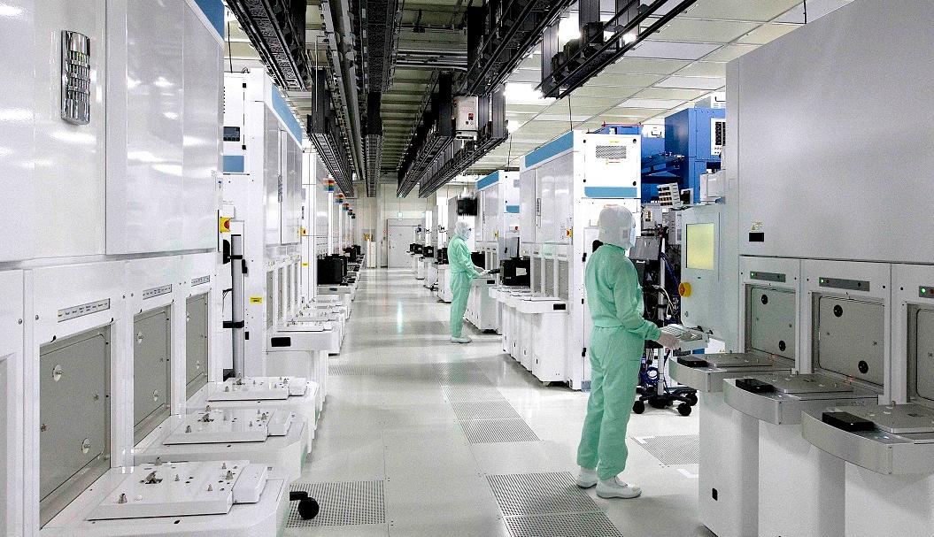
Unless Chinese chip manufacturers use household equipment directly from the device process development stage, such devices will use household equipment in large quantities. But there's another problem right away. At this stage, the performance of domestic equipment must meet basic requirements, and there must be sufficient trust among domestic chip manufacturers. In a real situation, with little R&D investment in home devices and a lack of opportunity for trial and error, it is unlikely that chipmakers will do so if such an obvious or real problem exists. In a production line that has been mass-produced. Helping home devices navigate the time-consuming and costly trial-and-error process. In this regard, it is unscientific. Therefore, as time passes, this complex problem remains. As long as it is possible to import equipment, there will not be many opportunities for household semiconductor equipment. This is the current situation faced by household equipment at this stage.
Semiconductor equipment and process integration
In the 1980s, purchased semiconductor equipment (such as etching machines) was only responsible for the hardware functions of the equipment, such as etching rate and etching uniformity. After purchasing the equipment, customers must develop their own process technology to meet the needs of mass production equipment. As a result, the problem is serious because it is almost impossible to develop process technology solely by customers without the cooperation of equipment manufacturers, so this often slows down the mass production of equipment.
As the demand for equipment and technology integration continues to increase to promote the advancement of the semiconductor industry. The equipment industry has taken a very difficult first step. It began researching and developing ways to implement this process on devices. It is known that these two disciplines require different talents. At the same time, a process test line must be established. However, process test lines must be maintained from the time the equipment is purchased to the operation and maintenance of the test lines. The cost of these aspects is high, but it is a difficult road that equipment manufacturers finally pass. The equipment sold today is an implementation of a specific process that is immediately ready for use on a customer's production line. It flows throughout the chip production line. The success of the thin film has ensured that the value of semiconductor equipment has increased from hundreds of thousands of dollars per unit to millions of dollars or more, reflecting its value. This is also a reflection of the cross-border success of the semiconductor equipment industry.
Opportunities for trial and error
The research and development process of semiconductor equipment must start with a prototype, which, after extensive modifications, will gradually become a product for sale. As with any new product, a process of trial and error is required because the starting prototype must have more glitches. Setting aside the minimum requirements for conventional equipment, the average MTBF time between failures is greater than 200 and requires trial and error. The problem was discovered and many modifications were made to meet the factory requirements of the equipment. .
But the issue of providing opportunities for trial and error is more complex, involving the respective interests of device makers and chipmakers.
From the perspective of domestic equipment manufacturers, there are two requirements: First, the current status of the industry. Equipment manufacturers are still unable to establish their own process test lines and lack semiconductor process capabilities and talents. The second is to support and trust the localization of devices. Give enough chance.
However, from the perspective of chip manufacturers, on the one hand, the prototype equipment provided should first reach an almost usable state, and on the other hand, the debugging of the equipment requires a lot of manpower, financial and material resources. This cost is high. Chip manufacturers shouldn't use it. endure endure endure.
This contradiction can be resolved abroad. Typically, those large equipment manufacturers will build their own part of the process test line. It has two functions. One is that customers can use their intermediate process silicon wafers to implement the next process and validate the device. Practicality, such as the requirement to achieve an aspect ratio of 1:100 for dielectric etching, and another home-grown device for trial and error processing, etc. The equipment ordering process for foreign customers often depends on the realization of a specific type of equipment. process. Therefore, it is necessary for equipment manufacturers to establish their own partial process test lines.
Nowadays, household equipment has moved up several steps, and it is well proven at least in industries such as photovoltaic and LED. However, localization of integrated circuit devices is still insufficient, but the quality has improved.
Therefore, in order to solve the problem of providing trial and error opportunities, it may be necessary to establish a process test line mainly supported by state funding, so that domestic semiconductor equipment, materials, etc. can first pass the qualification certification of testing. production line, and then enter the qualified chip production line to pass. Only in this way can the evaluation of mass production be entered into the order of equipment purchase in the chip production line.
Obviously, the working mode of this process test line needs to be explored, why it cannot be broken down for such a long time, but it must be continuously improved and continuously improved.
Accelerate localization
At this stage, the development of China's semiconductor industry, which mainly relies on imported equipment and materials, is still continuing and is desirable. However, the United States continues to use the "Entity List" and the "Wassenaar Treaty" to control exports, which has placed checks and balances on the development of China's semiconductor industry. The lesson that others cannot govern themselves is impressive.
Judging from the development of China's semiconductor industry, as long as imported equipment can continue to develop, the industry may still want to maintain the status quo. Like Ren Zhengfei, only a few people have the vision and sense of crisis. Because having "guts" is first, but having strength is more important. In addition, the year-on-year increase in the number of integrated circuits imported from China also reflects that China cannot do without the support of globalization.
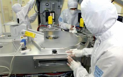
Because for Chinese chipmakers, they are used to imported equipment models that are relatively easy to run. For some device makers, they acknowledge the gap and believe the status quo will be more durable, which will help them catch up. On the contrary, when localization approaches, the pressure on equipment manufacturers will be greater.
Therefore, satisfying the status quo and being cautious about localization of equipment may be the mainstream thinking at this stage. I believe that only when U.S. export policies tighten and domestic chip production lines feel the pressure, making equipment localization an agenda, will the industry as a whole feel a sense of urgency. It may be the status quo and convoluted mentality. Therefore, at this stage of this once-in-a-lifetime opportunity, we must seize it firmly.
Facing the "pain points" in the development of the industry, there is no shrinking or fluke, only facing it bravely. Although the difficulty is great, it involves basic issues such as industrial base, but it must start from one step and recruit excellent domestic troops in a planned way to overcome the difficulty.
Therefore, first of all, we must not lose faith. We must have complete faith in our abilities. China's semiconductor industry is in a specific environment and has its own advantages and disadvantages. Its advantages can be supported by state funds and the huge Chinese market. Moreover, in times of crisis, China can have a unified will and unity. The disadvantage is that the West has been unable to understand it and is very worried that the strength of China's semiconductor industry will exceed theirs. Therefore, it does everything it can to suppress the development of China's semiconductor industry and prevent us from participating in globalization.
We must believe that globalization and localization are two different paths, which are crucial to the development of China's semiconductor industry at this stage. Our policy is to make the best possible use of globalization while never giving up on localization. . Although localization is difficult and expensive, it is one of the effective means to improve competitiveness. Obviously, we have to be confident. I believe that China's semiconductor industry will be able to overcome various difficulties and obstacles through partial localization efforts and break the Western ban. The "gap" of luck is when China's semiconductor industry develops and must wake up.
Disclaimer: This article is reproduced from the Internet and supports the protection of intellectual property rights. Please indicate the original source and author when reprinting. If there is any infringement, please contact us to delete it.
Company phone number: +86-0755-83044319
Fax/FAX: +86-0755-83975897
Email: 1615456225@qq.com
QQ: 3518641314 Manager Li
QQ: 332496225 Manager Qiu
Address: Room 809, Building C, Zhantao Technology Building, No. 1079 Minzhi Avenue, Longhua New District, Shenzhen
Related Recommendations
Exclusive Interview with Li Gang of Yunfan Ruida: The Precision of Millimeter-Wave Radar Products and the Warmth of Humanity
2026-07-22
2503
RF Passion, Craftsman’s Journey: Over 30 Years of Steadfast Dedication — Interview with Kinghelm Chief Engineer Mr. Qin hongxiang
2026-06-26
2676





 粤公网安备44030002007346号