
























Service Hotline
News

News
Intel accelerates process technology and packaging technology innovation
2022-03-17
659
● Intel’s process technology and packaging technology innovation roadmap injects power into the next wave of products from now to 2025 and beyond.
● Two breakthrough process technologies: Intel’s first new transistor architecture, RibbonFET, launched in more than a decade, and the industry’s first backside power transmission network, PowerVia.
● As Intel enters the semiconductor angstrom era, the updated node naming system will create a consistent framework to help customers and the industry establish a more accurate understanding of process node evolution.
● Intel Foundry Services (IFS) has strong momentum and announced the list of cooperative customers for the first time.

On July 27, 2021, Intel CEO Pat Gelsinger delivered a speech at the "Intel Accelerating Innovation: Process Technology and Packaging Technology Online Conference". In this online conference, Intel proposed a roadmap for future process technology and packaging technology. (Image source: Intel)
Today, Intel Corporation today announced the company’s most detailed process and packaging technology roadmap ever, demonstrating a series of underlying technology innovations that will continue to drive new product development from now to 2025 and beyond. In addition to unveiling its first new transistor architecture in more than a decade, RibbonFET, and the industry's first new backside power delivery network, PowerVia, Intel also highlighted plans to rapidly adopt the next generation of extreme ultraviolet lithography (EUV) technology, namely high numerical aperture (High-NA) EUV. Intel is expected to be the first to obtain the industry's first High-NA EUV lithography machine.
Building on Intel's unquestioned leadership in advanced packaging, we are accelerating our roadmap for process innovation to ensure that process performance once again leads the industry by 2025. Intel is leveraging our unparalleled drive for continuous innovation to deliver technology advancements from the transistor to the system level. Until the periodic table is exhausted, we will continue to pursue Moore's Law and continue to harness the magical power of silicon to advance innovation.
——Pat Kissinger
CEO of Intel Corporation
The industry has long realized that since 1997, the traditional nanometer-based naming method of process nodes no longer corresponds to the actual gate length of the transistor. Today, Intel has introduced a new naming system for its process nodes, creating a clear and consistent framework to help customers establish a more accurate understanding of the evolution of process nodes across the industry. With the launch of Intel Foundry Services (IFS), it is more important than ever to provide customers with clarity. Gelsinger said: "The innovative technologies announced today not only help Intel plan its product roadmap, but are also critical to our foundry services customers. There is strong interest in Intel Foundry Services (IFS) from the industry, and today I am pleased that we announced two important customers for our first cooperation. Intel Foundry Services has set sail!"
Intel technical experts detailed the following roadmap, which includes new node nomenclature and innovative technologies enabling each process node:
● Based on FinFET transistor optimization, Intel 7 will increase performance per watt by approximately 10%-15% compared to Intel 10nm SuperFin.The Alder Lake client products to be launched in 2021 will use the Intel 7 process, followed by Sapphire Rapids for data centers, which is expected to be put into production in the first quarter of 2022.
● Intel 4 completely adopts EUV lithography technology, which can use ultra-short wavelength light to engrave extremely small patterns.With about a 20% increase in performance per watt and improvements in chip area, Intel 4 will go into production in the second half of 2022 and ship in 2023. These products include Meteor Lake for clients and Granite Rapids for data centers.
● With the further optimization of FinFET and the increased use of EUV in more processes, Intel 3 will achieve an improvement of about 18% in performance per watt compared to Intel 4, and there will also be additional improvements in chip area.Intel 3 will be used in related product production starting in the second half of 2023.
● Intel 20A will usher in the Amy era with its two breakthrough technologies, RibbonFET and PowerVia.RibbonFET is Intel's implementation of the Gate All Around transistor and will be the company's first new transistor architecture since it pioneered FinFET in 2011. The technology speeds up transistor switching while achieving the same drive current as multi-fin structures, but taking up less space. PowerVia is Intel's unique, industry-first backside power transmission network that optimizes signal transmission by eliminating the need for front-side power supply wiring on the wafer. Intel 20A is expected to launch in 2024.Intel is also pleased to cooperate with Qualcomm on Intel 20A process technology.
● 2025 and beyond: The Intel 18A node, a step up from Intel 20A, is also under development and will be launched in early 2025. It will improve RibbonFET and achieve another major leap in transistor performance.Intel is also committed to defining, building and deploying the next generation of High-NA EUV, and is expected to be the first to obtain the industry's first High-NA EUV lithography machine. Intel is working closely with ASML to ensure the success of this industry-breaking technology beyond current generation EUV.
Dr. Ann Kelleher, senior vice president and general manager of technology development at Intel, said: "Intel has a long history of fundamental innovations in process technology that have driven industry leaps. We led the transition from 90nm strained silicon to 45nm high-K metal gates and were the first to introduce FinFET at 22nm. With two groundbreaking technologies, RibbonFET and PowerVia, Intel 20A will become another watershed in process technology."
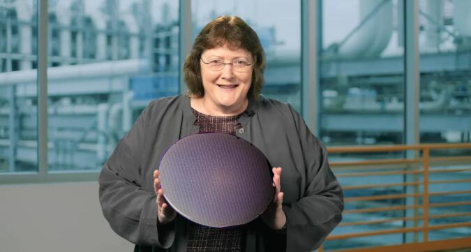
Dr. Ann Kelleher, senior vice president and general manager of technology development at Intel
With the implementation of Intel's new IDM 2.0 strategy, packaging becomes even more important to realizing the benefits of Moore's Law.Intel announced that AWS will be the first customer to use Intel Foundry Services (IFS) packaging solutions.Intel’s industry-leading advanced packaging roadmap proposes:
● EMIB will continue to lead the industry as the first 2.5D embedded bridge solution, and Intel has been shipping EMIB products since 2017.Sapphire Rapids will be the first Intel to adopt EMIB (Embedded Multi-die Interconnect Bridge) for volume shipments®Xeon®Data center products. It will also be the first in the industry to offer nearly the same performance as a monolithic design, but integrate two mask sizes. Following Sapphire Rapids, the bump pitch of the next generation EMIB will be shortened from 55 microns to 45 microns.
● Foveros leverages wafer-level packaging capabilities to provide the first-ever 3D stacking solution.Meteor Lake is the second generation deployment of Foveros technology implemented in client products. This product has a bump pitch of 36 microns, different chips can be based on multiple process nodes, and the thermal design power range is 5-125W.
● Foveros Omni pioneers the next generation of Foveros technology, providing unlimited flexibility for die-to-die interconnect and modular design through high-performance 3D stacking technology.Foveros Omni allows die disassembly to mix and match multiple top wafers with multiple substrates based on different wafer process nodes. It is expected to be used in mass-produced products in 2023.
● Foveros Direct enables the shift to direct copper-to-copper bonding, which enables low-resistance interconnects and makes the line between the two less distinct from wafer fabrication to packaging.Foveros Direct achieves sub-10 micron bump pitches, increasing the interconnect density of 3D stacks by an order of magnitude and proposing new concepts for functional die partitioning that was previously unachievable. Foveros Direct is a complement to Foveros Omni and is expected to be used in mass-produced products in 2023.
The breakthrough technologies discussed today are primarily developed at Intel's facilities in Oregon and Arizona, cementing Intel's position as the only U.S. leader with both chip R&D and manufacturing capabilities. Additionally, these innovations benefit from close collaboration with an ecosystem of US and European partners. Deep partnerships are key to moving fundamental innovations from laboratory research to mass manufacturing, and Intel is committed to working with governments everywhere to strengthen supply chains and advance economic and national security.
At the end of the online conference, Intel announced that it would hold an "Intel Innovation" summit and announced more relevant details. The "Intel Innovation" Summit will be held offline and online in San Francisco from October 27th to 28th, 2021.
Disclaimer: This article is reproduced from "ZhiIN". This article only represents the author's personal views and does not represent the views of Sacco Micro and the industry. It is only for reprinting and sharing to support the protection of intellectual property rights. Please indicate the original source and author for reprinting. If there is any infringement, please contact us to delete it.
Company phone number: +86-0755-83044319
Fax/FAX: +86-0755-83975897
Email: 1615456225@qq.com
QQ: 3518641314 Manager Li
QQ: 332496225 Manager Qiu
Address: Room 809, Building C, Zhantao Technology Building, No. 1079 Minzhi Avenue, Longhua New District, Shenzhen
Related Recommendations
Exclusive Interview with Li Gang of Yunfan Ruida: The Precision of Millimeter-Wave Radar Products and the Warmth of Humanity
2026-07-22
2563
RF Passion, Craftsman’s Journey: Over 30 Years of Steadfast Dedication — Interview with Kinghelm Chief Engineer Mr. Qin hongxiang
2026-06-26
2726





 粤公网安备44030002007346号