
























Service Hotline
News

News
What equipment is used in semiconductor production?
2022-03-16
1299
The semiconductor industry has surpassed the traditional steel industry and automobile industry and has become a high value-added, high-tech industry in the 21st century. Semiconductors are the core of many industrial equipment and are widely used in core fields such as computers, consumer electronics, network communications, and automotive electronics.
Semiconductors mainly have four components: integrated circuits, optoelectronic equipment, discrete equipment and sensors; integrated circuits are the core of the semiconductor industry, accounting for more than 80%. Integrated circuits include logic chips, memory chips, analog chips, MPUs, etc. The rapid development of integrated circuits in terms of performance, integration, and speed is based on the development of semiconductor physics, semiconductor devices, and semiconductor manufacturing processes.
The semiconductor industry has such a huge market, and semiconductor process equipment provides the manufacturing foundation for large-scale semiconductor manufacturing. In the future, semiconductor devices will be more integrated and miniaturized and more powerful. Attached below are the main equipment in the semiconductor production process.
1 Single crystal furnace
Equipment functions: melt semiconductor materials, pull single crystals, and provide single crystal semiconductor blanks for subsequent semiconductor device manufacturing.
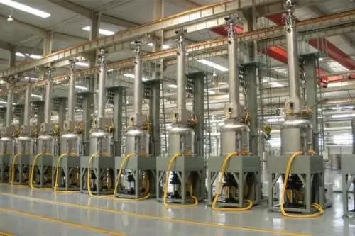
Main companies (brands):
International: German PVA TePla AG company, Japanese Ferrotec company, American QUANTUM DESIGN company, German Gero company, American KAYEX company.
Domestic: Beijing Jingyuntong, Qixing Huachuang, Beijing Jingyi Century, Hebei Jinglong Sunshine, Xi'an University of Science and Technology Jinko, Changzhou Huasheng Tianlong, Shanghai Hanhong, Xi'an Huade, China Electronics Technology Group 48th Institute, Shanghai Shenhe Thermal Magnetic.
2 Vapor phase epitaxy furnace
Equipment function: Provide a specific process environment for vapor phase epitaxy growth, realize the growth of thin-layer crystals on single crystals that have a corresponding relationship with the crystal phase of the single crystal, and make basic preparations for the functionalization of single crystal bottom deposition. Vapor phase epitaxy is a special process of chemical vapor deposition. The crystal structure of the thin layer grown is a continuation of the single crystal substrate and maintains a corresponding relationship with the crystal orientation of the substrate.
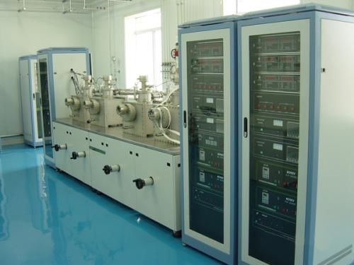
Main companies (brands):
International: American CVD Equipment Company, American GT Company, French Soitec Company, French AS Company, American Proto Flex Company, American Kurt J. Lesker Company, American Applied Materials Company.
Domestic: The 48th Institute of China Electronics Technology Group, Qingdao Serida, Hefei Kejing Materials Technology Co., Ltd., Beijing Jinsheng Micro-Nano, Jinan Liguan Electronic Technology Co., Ltd.
3 Molecular beam epitaxy system
Equipment functions: Molecular beam epitaxy system provides process equipment for growing thin films according to specific conditions on the surface of the substrate; molecular beam epitaxy is a technology for preparing single crystal thin films. It grows thin films layer by layer along the crystal axis direction of the substrate material under appropriate substrates and suitable conditions.
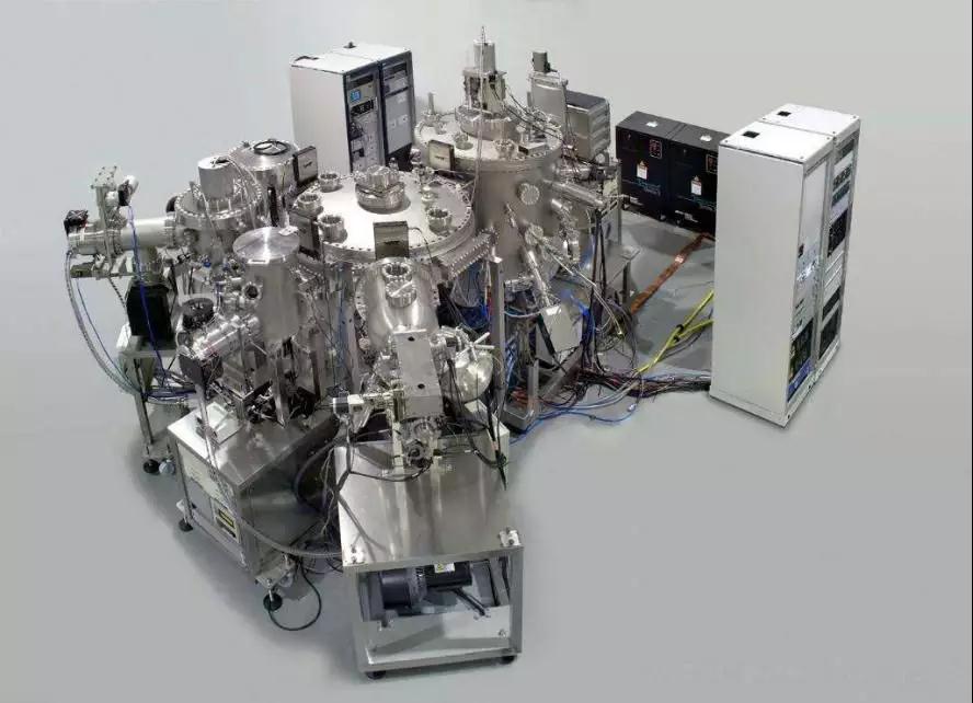
Main companies (brands):
International: French Riber Company, American Veeco Company, Finnish DCA Instruments Company, American SVT Associates Company, American NBM Company, German Omicron Company, German MBE-Komponenten Company, British Oxford Applied Research (OAR) Company.
Domestic: Shenyang Zhongke Instrument, Beijing Huidexin Technology Co., Ltd., Shaoxing Kuangtai Instrument Equipment Co., Ltd., Shenyang Keyou Vacuum Technology Co., Ltd.
4 Oxidation Furnace (VDF)
Equipment function: oxidize semiconductor materials, provide the required oxidation atmosphere, and realize the oxidation process of the semiconductor as expected. It is an indispensable link in the semiconductor processing process.
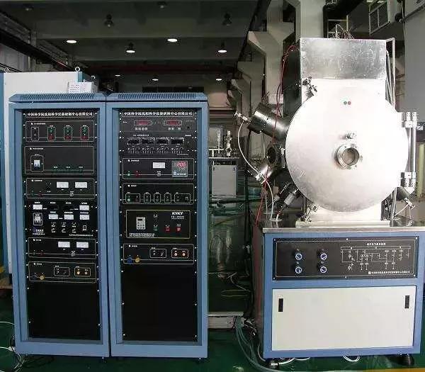
Main companies (brands):
International: British Thermco Company, German Centrotherm thermal solutions GmbH Co.KG Company.
Domestic: Beijing Qixing Huachuang, Qingdao Furunde, China Electronics Technology Group 48th Institute, Qingdao Xuguang Instrument Equipment Co., Ltd., China Electronics Technology Group 45th Institute.
5 Low-pressure chemical vapor deposition system (LPCVD)
Equipment function: Introduce the vapor containing the gaseous reagent or liquid reagent that constitutes the thin film elements and other gases required for the reaction into the reaction chamber of the LPCVD equipment, and a chemical reaction occurs on the substrate surface to generate a thin film.
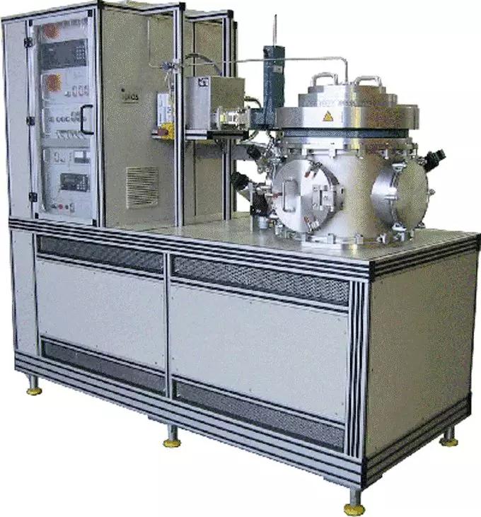
Main companies (brands):
International: Hitachi International Electric Co., Ltd. of Japan,
Domestic: Shanghai Chijian Semiconductor Technology Co., Ltd., China Electronics Technology Group 48th Institute, China Electronics Technology Group 45th Institute, Beijing Instrument Factory, Shanghai Machinery Factory.
6 Plasma enhanced chemical vapor deposition system (PECVD)
Equipment function: Use glow discharge in the deposition chamber to ionize it and then perform a chemical reaction on the substrate to deposit semiconductor thin film materials.
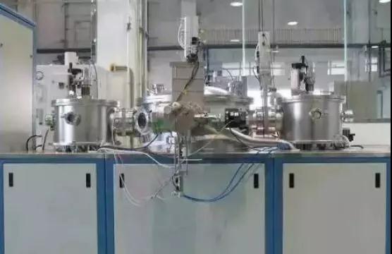
Main companies (brands):
International: American Proto Flex Company, Japanese Tokki Company, Japanese Shimadzu Company, American Lam Research Company, and Dutch ASM International Company.
Domestic: China Electronics Technology Group 45th Institute, Beijing Instrument Factory, Shanghai Machinery Factory.
7 Magnetron sputtering station (MSA)
Equipment function: Through a closed magnetic field parallel to the target surface during diode sputtering and the orthogonal electromagnetic field formed on the target surface, the secondary electrons are bound to a specific area on the target surface to achieve high ion density and high energy ionization, and the target atoms or molecules are sputtered and deposited on the substrate at a high rate to form a thin film.
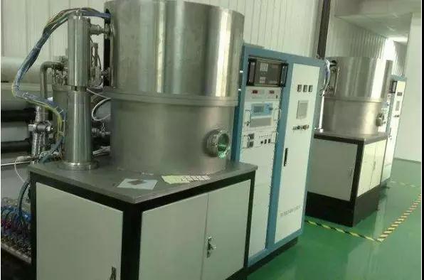
Main companies (brands):
International: American PVD Company, American Vaportech Company, American AMAT Company, Dutch Hauzer Company, British Teer Company, Swiss Platit Company, Swiss Balzers Company, German Cemecon Company.
Domestic: Beijing Instrument Factory, Shenyang Zhongke Instrument, Chengdu Nanguang Industrial Co., Ltd., China Electronics Technology Group 48th Institute, Core Equipment Co., Ltd., Shanghai Machinery Factory.
8 Chemical mechanical polishing machine (CMP)
Equipment function: Grinding and polishing the object to be ground (semiconductor) through the combined effects of mechanical grinding and chemical liquid dissolution and "corrosion".
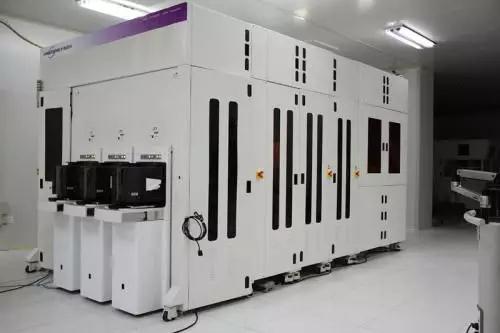
Main companies (brands):
International: American Applied Materials Company, American Novartis Systems Company, American Rtec Company.
Domestic: Lanzhou Lanxin High-tech Industry Co., Ltd., Elite Microelectronics.
9 Lithography machine
Equipment function: Apply glue on the surface of the semiconductor substrate (silicon wafer), transfer the pattern on the mask to the photoresist, and temporarily "copy" the device or circuit structure to the silicon wafer.
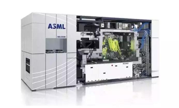
Main companies (brands):
International: ASML of the Netherlands, Lam Semiconductor Company of the United States, Nikon Company of Japan, Canon Company of Japan, ABM Company of the United States, SUSS Company of Germany, and MYCRO Company of the United States.
Domestic: The 48th Institute of China Electronics Technology Group, the 45th Institute of China Electronics Technology Group, Shanghai Machinery Factory, Chengdu Nanguang Industrial Co., Ltd.
10 Reactive ion etching system (RIE)
Equipment function: Apply high-frequency voltage between flat electrodes to generate an ion layer hundreds of microns thick. Place the pattern into the pattern, and the ions impact the pattern at high speed to achieve chemical reaction etching and physical impact, and realize the processing and molding of semiconductors.
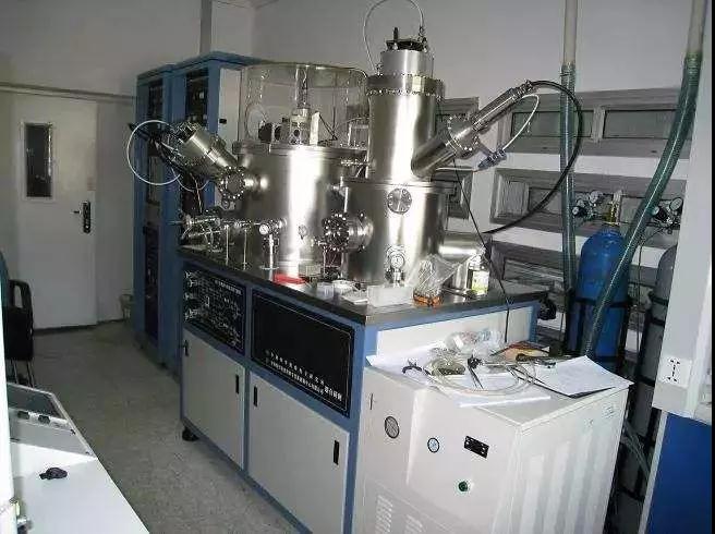
Main companies (brands):
International: Japan Evatech Company, American NANOmaster Company, Singapore REC Company, South Korea JuSung Company, South Korea TES Company.
Domestic: Beijing Instrument Factory, Beijing Qixing Huachuang Electronics Co., Ltd., Chengdu Nanguang Industrial Co., Ltd., and the 48th Institute of China Electronics Technology Group.
11 ICP plasma etching system
Equipment function: One or more gas atoms or molecules are mixed in the reaction chamber and form a plasma under the action of external energy (such as radio frequency, microwave, etc.). On the one hand, the active groups in the plasma react chemically with the surface material to be etched to generate volatile products; on the other hand, the ions in the plasma are guided and accelerated under the action of bias voltage, achieving directional corrosion and accelerated corrosion of the surface to be etched.
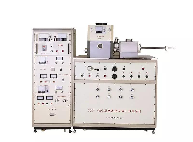
Main companies (brands):
International: Oxford Instruments Company of the United Kingdom, Torr Company of the United States, Gatan Company of the United States, Quorum Company of the United Kingdom, Leman Company of the United States, and Pelco Company of the United States.
Domestic: Beijing Instrument Factory, Beijing Qixing Huachuang Electronics Co., Ltd., China Electronics Technology Group 48th Institute, Godel Plasma Technology (Hong Kong) Holdings Co., Ltd., Institute of Microelectronics, Chinese Academy of Sciences, Northern Microelectronics, Beijing Oriental Zhongke Integrated Technology Co., Ltd., Beijing Chuangshi Weiner Technology.
12 Wet etching and cleaning machine
Equipment function: Wet etching is a technology that immerses etching materials in corrosive liquid for corrosion. Cleaning is to reduce contamination, because contamination will affect device performance, cause reliability problems, and reduce yield. This requires thorough cleaning before the next process of each layer or the next layer.
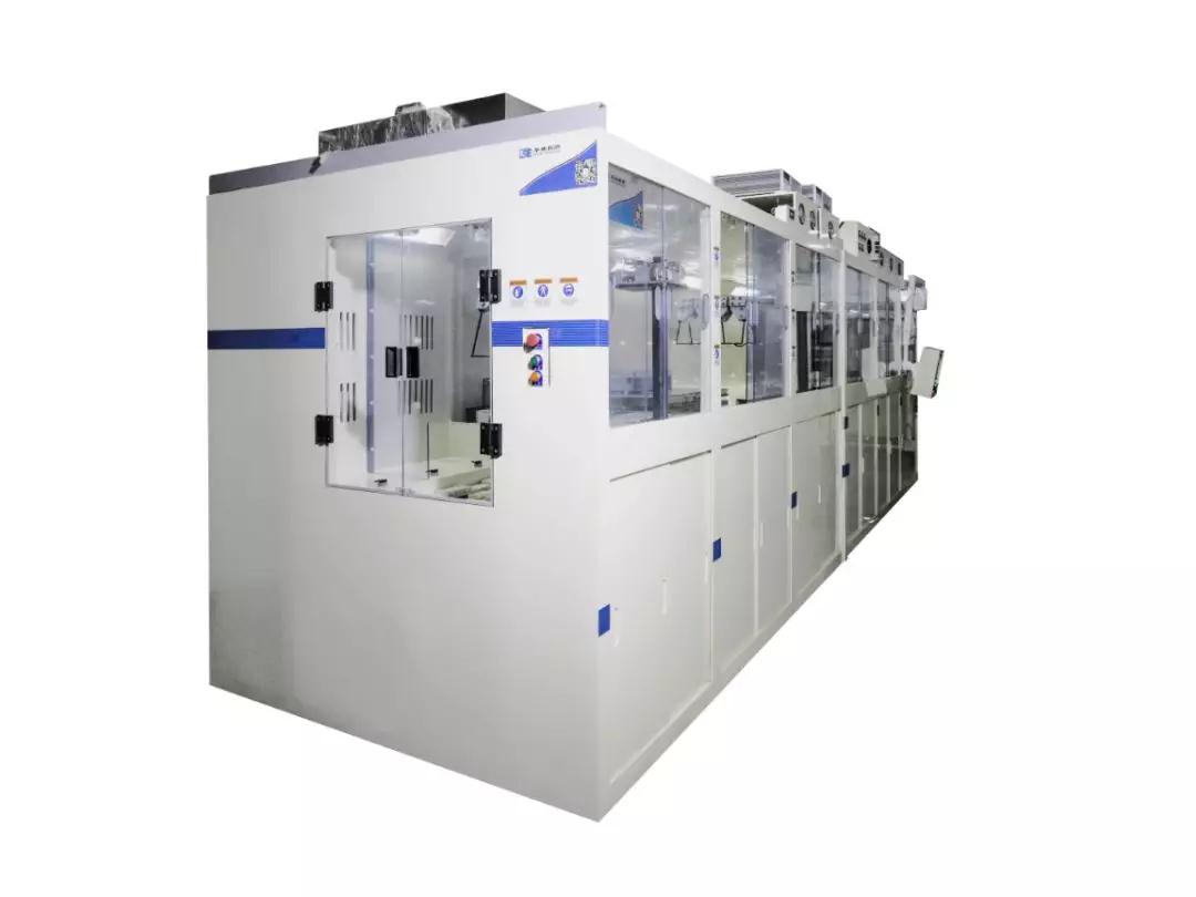
Main companies (brands):
International: Japan Screen, South Korea SEMES, Japan Tokyo Electron, and the United States Lam Research.
Domestic: Nantong Hualincona Semiconductor Equipment Co., Ltd., Beijing Qixing Huachuang Electronics Co., Ltd., China Electronics Technology Group 45th Institute, Taiwan Hongsu.
13 Ion implanter (IBI)
Device function: Doping the area near the semiconductor surface.
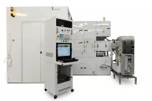
Main companies (brands):
International: American Varian Semiconductor Equipment Company, American CHA Company, American AMAT Company, Varian Semiconductor Manufacturing Equipment Company (acquired by AMAT).
Domestic: Beijing Instrument Factory, China Electronics Technology Group 48th Institute, Chengdu Nanguang Industrial Co., Ltd., Shenyang Fangji Light Industry Machinery Co., Ltd., Shanghai Silicon Tuo Microelectronics Co., Ltd.
14 probe test bench
Equipment function: Conduct electrical testing by contacting the probe with the pad of the semiconductor device to detect whether the performance indicators of the semiconductor meet the design performance requirements.
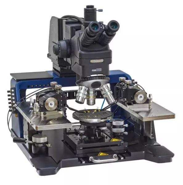
Main companies (brands):
International: German Ingun Company, American QA Company, American MicroXact Company, Korean Ecopia Company, Korean Leeno Company.
Domestic: The 45th Institute of China Electronics Technology Group, Beijing Qixing Huachuang Electronics Co., Ltd., Rico Instruments, Huarong Group, Shenzhen Semiconductor Technology.
15 wafer thinning machine
Equipment function: reduce the thickness of the wafer through polishing.
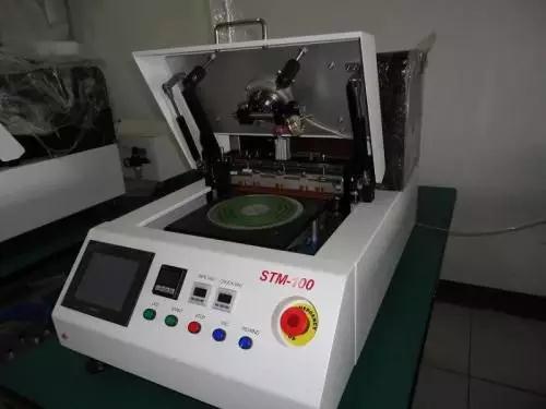
Main companies (brands):
International: Japanese DISCO Company, German G&N Company, Japanese OKAMOTO Company, Israeli Camtek Company.
Domestic: Lanzhou Lanxin High-tech Industry Co., Ltd., Shenzhen Fangda Grinding Equipment Manufacturing Co., Ltd., Shenzhen Jinlili Precision Grinding Machine Manufacturing Co., Ltd., Weianda Grinding Equipment Co., Ltd., Shenzhen Huanianfeng Technology Co., Ltd.
16 Wafer dicing machine (DS)
Equipment function: Die cutting the wafer into small pieces.
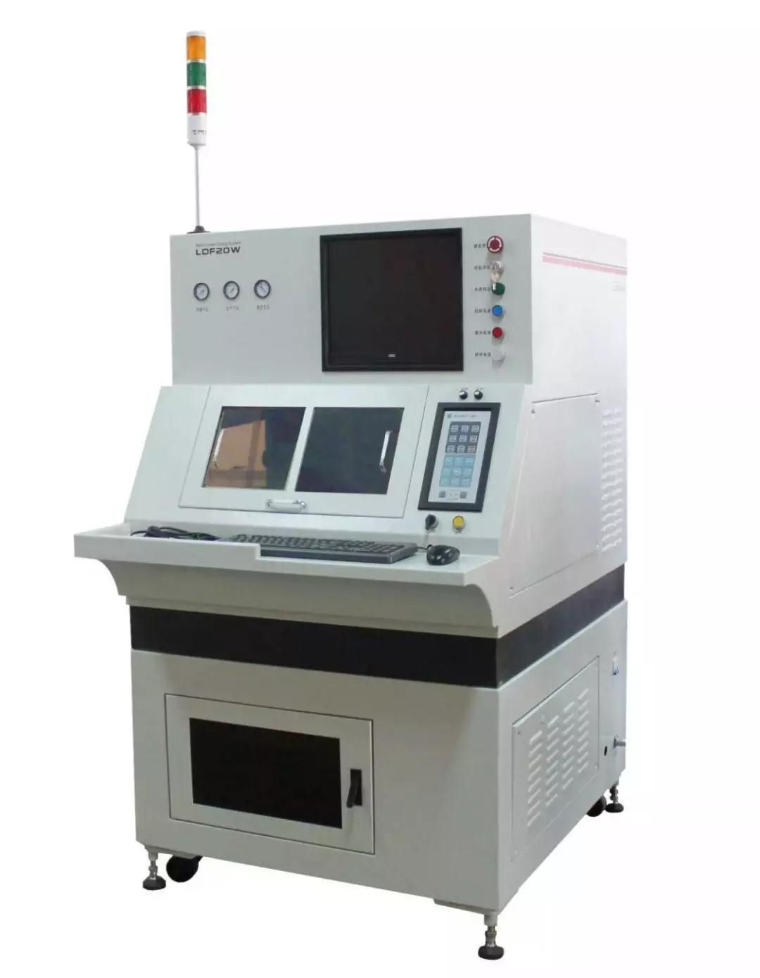
Main companies (brands):
International: German OEG Company, Japanese DISCO Company.
Domestic: The 45th Institute of China Electronics Technology Group, Beijing Kechuangyuan Optoelectronics Technology Co., Ltd., Shenyang Instrumentation Technology Research Institute, Northwest Machinery Co., Ltd. (formerly State-owned Northwest Machinery Factory 709 Factory), Huisheng Electronic and Electronic Machinery Equipment Co., Ltd., Lanzhou Lanxin High-tech Industry Co., Ltd., Han's Laser, Shenzhen Ruby Laser Equipment Co., Ltd., Wuhan Sangong, Zhuhai Lailian Optoelectronics, Zhuhai Yuemao Technology.
17 Wire Bonder
Equipment function: Connect the Pad on the semiconductor chip and the Pad on the pin with conductive metal wires (gold wire).
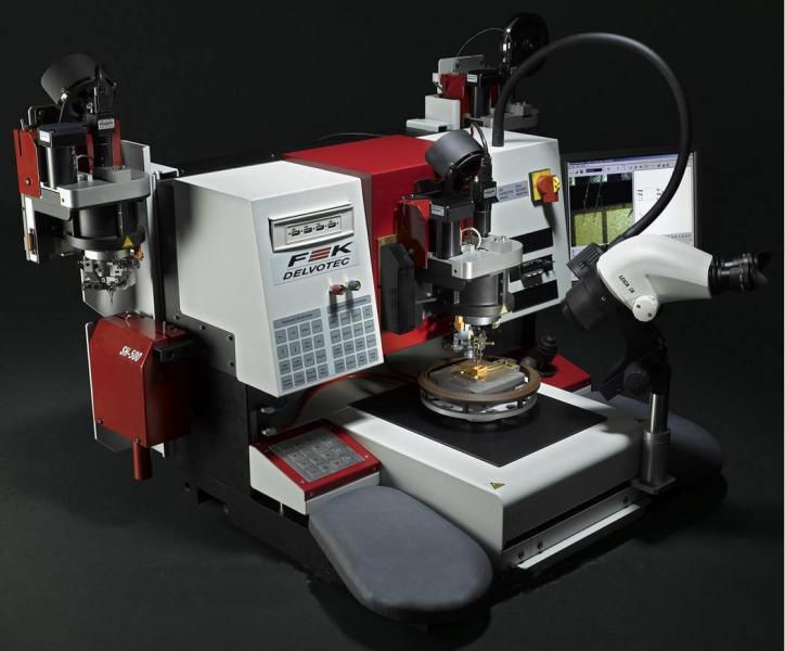
Main companies (brands):
International: American Aotei Company, German TPT Company, Austrian FK Company, and Malaysian UNISEM Company.
Domestic: The 45th Institute of China Electronics Technology Group, Beijing Chuangshijie Technology Development Co., Ltd., Yuxin (Chengdu) Integrated Circuit Packaging and Testing Co., Ltd. (Malaysian Unison Investment), Shenzhen Kaijiu Automation Equipment Co., Ltd.
Summary: For China's semiconductor industry to achieve a leap from tracking to leading, the equipment industry will be an important link. More innovation is needed to lead the development of China's semiconductor equipment and promote the leapfrog improvement of my country's chip process and technology.
Note: This article is reproduced from the Internet and supports the protection of intellectual property rights. Please indicate the original source and author when reprinting. If there is any infringement, please contact us to delete it.
Company phone number: +86-0755-83044319
Fax/FAX: +86-0755-83975897
Email: 1615456225@qq.com
QQ: 3518641314 Manager Li
QQ: 332496225 Manager Qiu
Address: Room 809, Building C, Zhantao Technology Building, No. 1079 Minzhi Avenue, Longhua New District, Shenzhen
Related Recommendations
Exclusive Interview with Li Gang of Yunfan Ruida: The Precision of Millimeter-Wave Radar Products and the Warmth of Humanity
2026-07-22
2468
RF Passion, Craftsman’s Journey: Over 30 Years of Steadfast Dedication — Interview with Kinghelm Chief Engineer Mr. Qin hongxiang
2026-06-26
2652





 粤公网安备44030002007346号