
























Service Hotline
News

News
"Advanced Packaging" is all covered in one article
2022-03-16
1082
Based on XY plane extension Advanced packaging technology
The XY plane here refers to the wafer or the XY plane of the chip. The distinctive feature of this type of package is that there is no TSV through silicon hole. The signal extension means or technology is mainly implemented through the RDL layer. There is usually no substrate. The RDL wiring is attached to the silicon body of the chip or on additional molding. Because the final packaged product does not have a substrate, such packages are relatively thin and are currently widely used in smartphones.
1.FOWLP
Before the emergence of WLP technology, the traditional packaging process steps were mainly carried out after cutting and slicing the die. The wafer was first cut and diced, and then packaged into various forms.
WLP came out around 2000. There are two types: Fan-in (fan-in) and Fan-out (fan-out). WLP wafer-level packaging is different from traditional packaging. In the packaging process, most of the process is to operate the wafer, that is, overall packaging (Packaging) is performed on the wafer, and after the packaging is completed, it is cut into slices. Because it is cut into pieces after packaging is completed, the size of the packaged chip is almost the same as that of the bare chip, so it is also called CSP (Chip Scale Package) or WLCSP (Wafer Level Chip Scale Packaging). This type of packaging conforms to the market trend of light, small, short, and thin consumer electronic products. The parasitic capacitance and inductance are relatively small, and it has the advantages of low cost and good heat dissipation.At first, WLP mostly adopted the Fan-in type, which can be called Fan-in WLP or FIWLP. It is mainly used in chips with smaller area and fewer pins.
As IC technology improves, the chip area shrinks, and the chip area cannot accommodate enough pins. Therefore, the Fan-Out WLP packaging form, also known as FOWLP, is derived, which makes full use of RDL for connections outside the chip area to obtain more pins.
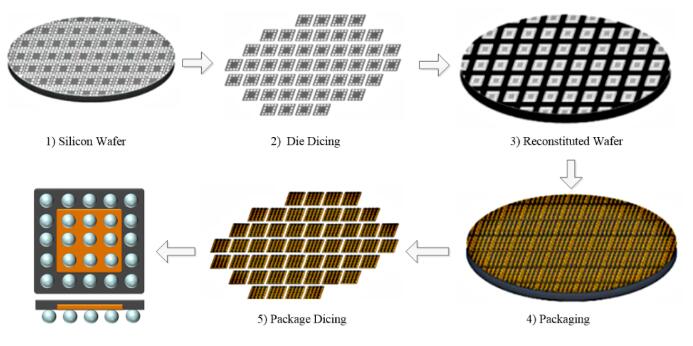
In FOWLP, since RDL and Bump are to be led out to the periphery of the bare chip, the bare chip wafer needs to be diced and segmented first, and then the independent bare chips are reconfigured into the wafer process. Based on this, through batch processing and metallized wiring interconnection, the final package is formed. The FOWLP encapsulation process is shown in the figure below.
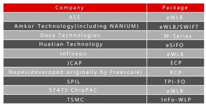
FOWLP is supported by many companies, and different companies have different naming methods. The figure below shows the FOWLP provided by major companies.
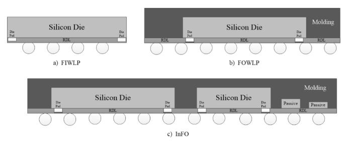
 Whether using Fan-in or Fan-out, the connection between WLP wafer-level packaging and PCB is in the form of flip chip. The active side of the chip faces down towards the printed circuit board, which can achieve the shortest electrical path, which also ensures higher speed and less parasitic effects. On the other hand, due to the use of batch packaging, the entire wafer can be packaged at once, and cost reduction is another driving force for wafer-level packaging. 2.INFOInFO (Integrated Fan-out) is an advanced FOWLP packaging technology developed by TSMC in 2017. It is an integration of the FOWLP process and can be understood as the integration of multiple chip Fan-Out processes, while FOWLP focuses on the Fan-Out packaging process itself. InFO gives space for multiple chip integration and can be applied to the packaging of radio frequency and wireless chips, processor and baseband chip packaging, graphics processors and network chips. The figure below is a comparison diagram of FIWLP, FOWLP and InFO.
Apple's iPhone processors have been produced by Samsung in the early years, but TSMC has taken orders for two generations of iPhone processors, starting with the Apple A11. One of the keys is TSMC's new packaging technology InFO, which allows chips to be directly interconnected, reducing thickness and freeing up valuable space for batteries or other parts.
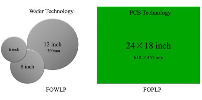
Apple started using InFO packaging with the iPhone 7 and will continue to use it. iPhone 8, iPhone X, and other mobile phone brands in the future will also begin to use this technology. The joining of Apple and TSMC has changed the application status of FOWLP technology and will enable the market to gradually accept and widely apply FOWLP (InFO) packaging technology. 3.FOPLPFOPLP (Fan-out Panel Level Package) panel-level packaging draws on the ideas and technology of FOWLP, but uses a larger panel, so it can mass-produce packaged products several times that of 300 mm silicon wafer chips. FOPLP technology is an extension of FOWLP technology. It performs the Fan-Out process on a larger square carrier board, so it is called FOPLP packaging technology. The Panel carrier board can be a PCB carrier board or a glass carrier board for LCD panels. Currently, FOPLP uses a 24-18-inch (610-457mm) PCB carrier board, whose area is about 4 times that of a 300 mm silicon wafer. Therefore, it can be simply regarded as a single process that can mass-produce advanced packaging products that are 4 times the size of a 300 mm silicon wafer. Like the FOWLP process, FOPLP technology can integrate the front-end and back-end processes of packaging. It can be regarded as a one-time packaging process, so it can significantly reduce production and material costs. The picture below shows the comparison between FOWLP and FOPLP.
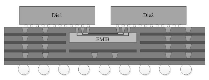
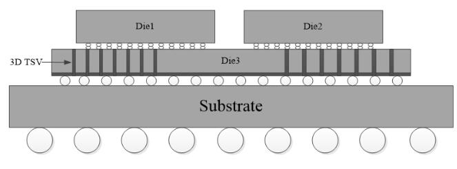
Compared with silicon interposers, EMIB silicon wafers are smaller, more flexible, and more economical. EMIB packaging technology can package CPU, IO, GPU and even FPGA, AI and other chips together as needed. It can package chips of 10nm, 14nm, 22nm and other different processes together into a single chip to meet the needs of flexible business.
Through EMIB, the KBL-G platform integrates Intel Core processors and AMD Radeon RX Vega M GPUs. It combines the powerful computing capabilities of Intel processors with the excellent graphics capabilities of AMD GPUs, and has an excellent cooling experience. This chip made history and brought product experience to a new level.
Based on Z-axis extension Advanced packaging technology
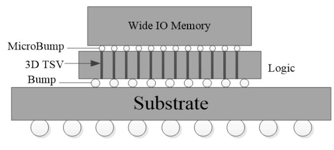
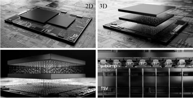
Advanced packaging technology based on Z-axis extension mainly uses TSV for signal extension and interconnection. TSV can be divided into 2.5D TSV and 3D TSV. Through TSV technology, multiple chips can be vertically stacked and interconnected.
In 3D TSV technology, chips are very close to each other, so there will be less delay. In addition, the shortened interconnect length can reduce related parasitic effects, allowing the device to run at higher frequencies, which translates into performance improvements and greater cost reductions. TSV technology is a key technology for three-dimensional packaging. Research institutions including semiconductor integrated manufacturers, integrated circuit manufacturing foundries, packaging foundries, emerging technology developers, universities and research institutes, and technology alliances have conducted various research and development on TSV processes. In addition, readers need to note that although advanced packaging technology based on Z-axis extension mainly performs signal extension and interconnection through TSV, RDL is also indispensable. For example, if the TSVs of the upper and lower chips cannot be aligned, local interconnection through RDL is required. 5.CoWoSCoWoS (Chip-on-Wafer-on-Substrate) is a 2.5D packaging technology launched by TSMC. CoWoS packages the chip onto a silicon adapter board (interposer), uses high-density wiring on the silicon adapter board for interconnection, and then installs it on the packaging substrate, as shown in the figure below.
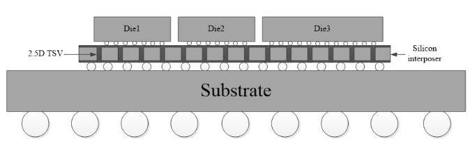
TSMC began mass production of CoWoS in 2012. Through this technology, multiple chips are packaged together and interconnected through high-density Silicon Interposer, achieving the effects of small package size, high performance, low power consumption, and fewer pins.
CoWoS technology is widely used. Nvidia's GP100 and the Google chip TPU2.0 behind AlphaGo that defeated Ke Jie all use CoWoS technology. Artificial intelligence AI also has CoWoS contributions. Currently, CoWoS has received support from high-end chip manufacturers such as NVIDIA, AMD, Google, XilinX, and Huawei HiSilicon.
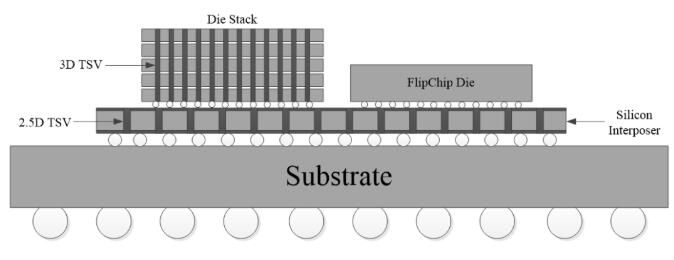
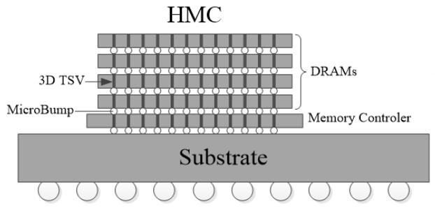
6.HBMHBM (High-Bandwidth Memory) high-bandwidth memory, mainly targeted at the high-end graphics card market. HBM uses 3D TSV and 2.5D TSV technology to stack multiple memory chips together through 3D TSV, and uses 2.5D TSV technology to interconnect stacked memory chips and GPUs on the carrier board. The figure below shows a schematic diagram of HBM technology.
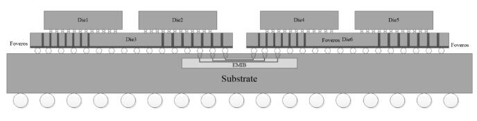
Co-EMIB packaging technology can provide performance comparable to that of a single chip. The key to achieving this technology is ODI (Omni-Directional Interconnect) omnidirectional interconnection technology. ODI has two different types. In addition to elevator-type connections that connect different layers, there are also overpasses that connect different three-dimensional structures, as well as mezzanines between layers, allowing different chip combinations to have extremely high flexibility. ODI packaging technology allows chips to achieve both horizontal and vertical interconnections.
Co-EMIB uses a new 3D + 2D packaging method to change chip design thinking from the past flat puzzle to stacking blocks. Therefore, in addition to revolutionary new computing architectures such as quantum computing, CO-EMIB can be said to be the best practice in maintaining and continuing the existing computing architecture and ecosystem.11.SoIC
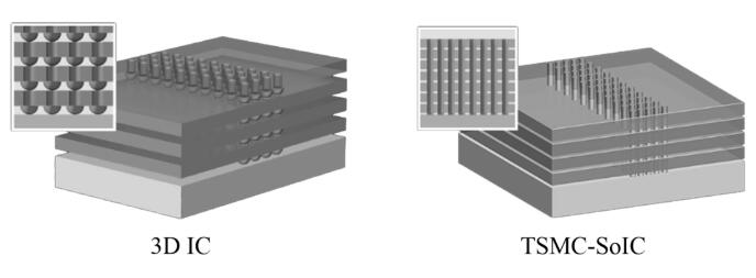
SoIC, also known as TSMC-SoIC, is a new technology proposed by TSMC - System-on-Integrated-Chips. It is expected that TSMC's SoIC technology will be mass-produced in 2021. What exactly is SoIC? The so-called SoIC is an innovative multi-chip stack technology that can integrate processes at the wafer level below 10 nanometers. The most distinctive feature of this technology is the no-bump bonding structure, which results in higher integration density and better operating performance. SoIC includes two technical forms: CoW (Chip-on-wafer) and WoW (Wafer-on-wafer). From the description of TSMC, SoIC is a direct bonding (Bonding) technology of WoW wafer to wafer or CoW chip to wafer, which belongs to Front-End 3D technology (FE 3D), while the aforementioned InFO and CoWoS belong to Back-End 3D technology (BE 3D). TSMC and Siemens EDA (Mentor) cooperate on SoIC technology and launch related design and verification tools. The figure below is a comparison of 3D IC and SoIC integration.
Summarize Advanced packaging technologyIn this article, we describe 12 of today’s most mainstream advanced packaging technologies. The following table is a horizontal comparison of these mainstream advanced packaging technologies.
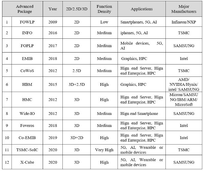
From the comparison, we can see that the emergence and rapid development of advanced packaging mainly occurred in the past 10 years. Its integration technology mainly includes 2D, 2.5D, 3D, 3D+2D, 3D+2.5D. The functional density also includes low, medium, high and extremely high. The application fields include It covers 5G, AI, wearable devices, mobile devices, high-performance servers, high-performance computing, high-performance graphics cards and other fields. The main application manufacturers include well-known chip manufacturers such as TSMC, Intel, and SAMSUNG, which also reflects the trend of integration of advanced packaging and chip manufacturing.
Finally, let us summarize: the purpose of advanced packaging is:
Improve functional density, shorten interconnection length, improve system performance, and reduce overall power consumption.
Advanced packaging also puts forward new requirements for EDA tools. EDA tools need to support FIWLP, FOWLP, 2.5DTSV and 3D TSV design, as well as multi-substrate design. Because the silicon interposer and packaging substrate (Substrate) are often integrated together in a product, major EDA companies have launched new tools to support the design and verification of advanced packaging, including Synopsys, Cadence, Siemens EDA (Mentor) is actively involved.
The figure below shows a screenshot of the advanced packaging design of Siemens EDA XPD tool. The design includes 3D TSV and 2.5D TSV design, Interposer, Substrate, FlipChip, Microbump, BGA and other elements, which are detailed and accurately reflected in the EDA tool. For detailed design methods of advanced packaging, please refer to the new book "Microsystems Based on SiP Technology" to be published in the near future.
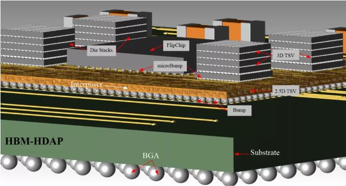
Typical advanced packaging design (Siemens EDA XPD design screenshot)
Disclaimer: This article is reproduced from "SiP and Advanced Packaging Technology", which supports the protection of intellectual property rights. Please indicate the original source and author of the reprint. If there is any infringement, please contact us to delete it.
Company phone number: +86-0755-83044319
Fax/FAX: +86-0755-83975897
Email: 1615456225@qq.com
QQ: 3518641314 Manager Li
QQ: 332496225 Manager Qiu
Address: Room 809, Building C, Zhantao Technology Building, No. 1079 Minzhi Avenue, Longhua New District, Shenzhen
Related Recommendations
Exclusive Interview with Li Gang of Yunfan Ruida: The Precision of Millimeter-Wave Radar Products and the Warmth of Humanity
2026-07-22
2516
RF Passion, Craftsman’s Journey: Over 30 Years of Steadfast Dedication — Interview with Kinghelm Chief Engineer Mr. Qin hongxiang
2026-06-26
2687





 粤公网安备44030002007346号