
























Service Hotline
News

News
Native I/O ESD protection for 28Gbps to 112Gbps SerDes interfaces in CMOS and FinFET processes
2022-03-16
804
summary:
To meet the demand for higher data throughput, semiconductor companies are developing faster wireless, wired and optical interfaces. It is mainly based on the implementation of BiCMOS, advanced CMOS technology and FinFET nodes in ESD sensitive circuits. However, the parasitic capacitance of traditional ESD solutions limits the signal frequency. This article describes the small-area, low-capacitance analog I/O used in TSMC 28nm CMOS and TSMC 16nm, 12nm, 7nm FinFET processes for high-speed SerDes (28Gbps to 112Gbps) circuits. The parasitic capacitance of ESD solutions is reduced to less than 100fF, and some applications in silicon photonics even reduce it to less than 20fF.
I.Introduction
In today's world, the demand for data transmission is increasing day by day. The amount of data people consume daily watching videos continues to increase. With the popularization of smartphones, computer applications, data centers and long-distance information exchanges, the demand for various bandwidths continues to grow. This demand in turn has driven the semiconductor industry to continue to develop and seek faster development of wireless, wired and optical interfaces. A few years ago, the speed limit was around 10 Gbps. Recently, circuits are running at 56Gbps or even 112Gbps.
For such high-speed communication interfaces, chip designers need to limit the parasitic capacitance of the on-chip ESD protection clamps connected to the interface. Since traditional ESD methods have shortcomings, special analog I/O circuits are required. This article demonstrates silicon-proven ESD solutions for TSMC 28nm in CMOS processes and TSMC 16nm, 12nm and 7nm in FinFET processes. The parasitic capacitance of ESD solutions is reduced to less than 100fF, and for some silicon photonics applications, it is even reduced to less than 20fF.
II. Traditional ESD methods
Figure 1 shows the traditional ESD method of simulating an I/O PAD module. It consists of a diode connecting Vss to the I/O PAD and a diode connecting the I/O PAD module to Vdd and a power/rail clamp between Vdd and Vss [1-5].
IC designers like it because these two diode designs are easy to implement and have a small silicon footprint and fairly low parasitic capacitance.
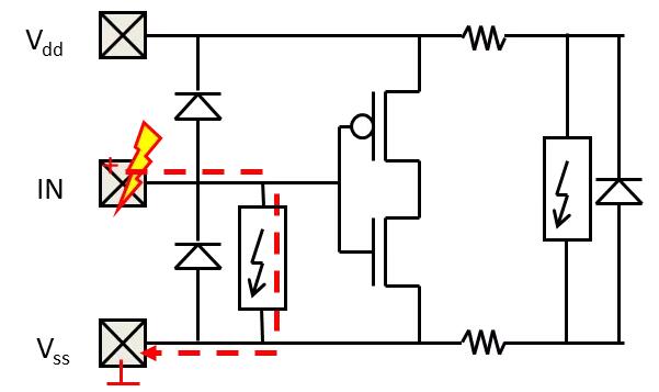
Figure 1: Traditional ESD methods applied to many I/O PAD modules: one diode from Vss to I/O and another diode from I/O to Vdd. One power clamp is used for the 1/2 stress combination.
For sensitive nodes, IC designers will add an isolation resistor between the I/O and the circuit to increase the ESD design window. If the functional circuit cannot handle electrostatic discharge (ESD) current, add a secondary clamp after the isolation resistor (Figure 2).
Figure 2: Sometimes, IC designers will add a resistor between the I/O PAD module and the circuit and place a small secondary clamp in front of the sensitive circuit. This increases the ESD design window.
There are several problems with this simple approach, especially with high-speed interfaces:
(1) Isolation resistance seriously affects high-speed operation and increases noise.
(2) ESD diodes may introduce excessive parasitic capacitance between the signal PAD and the power line.
(3) Due to noise coupling between PAD and Vdd or the signal voltage may be higher than the reference Vdd voltage, or due to matching issues, some interfaces cannot withstand the voltage stimulation caused by the diode from the I/O PAD module to Vdd.
(4) For sensitive nodes, the total voltage drop on the expected ESD current path may be higher than the fault voltage of the functional circuit [5].
An easy way to reduce capacitance (question 2) and increase voltage tolerance (question 3) is to use 2 or more diodes in series. However, this leads to higher voltage drops under ESD stress, thus worsening problem 4. In 2017, an alternative with a novel bipolar concept was proposed [6-7].
This article discusses a project in which the IC designer replaced the traditional dual-diode ESD approach with a local protection clamping concept, as shown in Figure 3. If functional operation cannot tolerate the diode going from "IN" to Vdd, it can be removed. This is typical for fail-safe, hot-plug, open-drain outputs, cold-standby inputs, or overvoltage-resistant interfaces [8].
Figure 3: Simplified circuit schematic using local clamp ESD protection. If functional operation is required, the diode between IN and Vdd can be removed. In some cases, another clamp is added between Vdd and "IN".
The local clamping method has many advantages:
(1) Reduce dependence on bus resistance
(2) The voltage drop under ESD conditions is greatly reduced without the need for isolation resistors, making it very suitable for sensitive nodes.
(3) Provides different options for reducing parasitic capacitance (see case study below)
(4) Each I/O PAD can be optimized separately. For example: Some PADs may require higher ESD tolerance, otherwise they cannot withstand the discharge of the diode between I/O and Vdd.
III.SerDes Protection Case Study
The following case study summarizes several local clamping methods with (ultra)low parasitic capacitance to protect high-speed SerDes interfaces ranging from 28nm CMOS to 7nm FinFET. Different types of SCR-based local clamping were used in the case study (Fig. 4). Diode triggered SCR and ESD-on-SCR were previously used to protect wireless LNA interfaces [9].
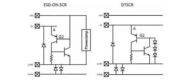
Figure 4: Two ESD protection clips used in the case study. Once the IO level raises the diode drop (Anode-G2) above the Vdd voltage, the Sofics ESD-on-SCR is triggered. Once AnodeG2 and the trigger diode are forward biased, the Sofics DTSCR turns on.
1.FPGA 28nm, 28Gbps SerDes
For a series of advanced FPGA products in TSMC’s 28nm process, customers require customized ESD protection units. The 28Gbps SerDes interface requires the following specifications:
-The parasitic capacitance is well below 100fF.
-ESD level: > 1kV HBM; > 250V CDM
A scaled-down version of the Sofics DTSCR clamp was chosen for local protection of the Tx and Rx interfaces. A secondary local CDM clamp is added behind the isolation resistor to protect the thin gate oxide in the Rx case (Figure 5). The parasitic capacitance of DTSCR, reverse diode and metal connections is kept below 80fF.
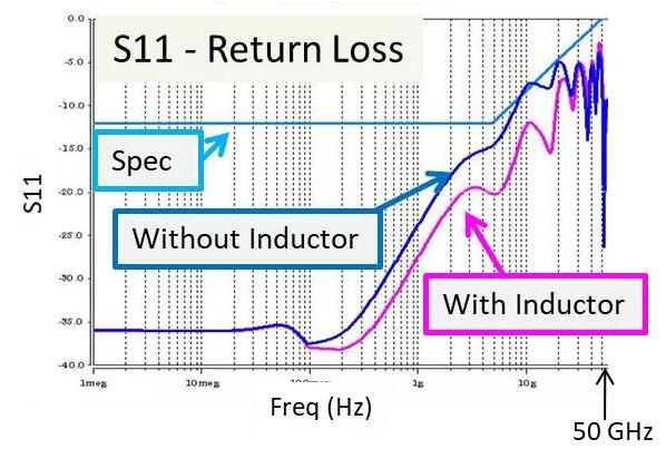
Figure 5: Schematic of the 28Gbps SerDes Rx (input) stage showing the DTSCR local clamping and secondary protection stages for enhanced CDM protection.
To meet the S11–Return Loss specification, an inductor is placed in series with the DTSCR (Figure 6). Comply with all specifications including CDM. The FPGA device reaches over 300V with a peak current of 4.5A. All analysis results have been presented at the IEW 2011 event [10].
Figure 6: To meet the S11 specification, an inductor is placed in series with the DTSCR. The coil reduces the S11 peak at 10 GHz and 20 GHz.
2. Universal SerDes 16nm, 28Gbps
High-speed (data center) communication chips with 28 Gbps SerDes in 16nm process require customized ESD protection solutions.
Local ESD clamps must meet these requirements:
- Protection of sensitive thin oxide 0.8V core transistors with fault voltage under ESD stress below 3.3V
-Low leakage ESD clamp, less than 10nA at high temperature (125°C)
-Small silicon footprint enables multiple channels on the same communications chip
-No resistor
- > 2kV HBM
-Maximum ESD junction capacitance is 100fF
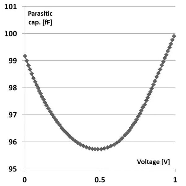
Figure 7: Schematic diagram of the protection concept of differential pairs of Tx interfaces. A local clamp and parallel reverse diode are added to both paths of the differential pair.
Based on extensive analysis of chips based on TSMC's 16nm FinFET technology, the ESD-on-SCR concept was chosen as the local clamping device. The TLP data is shown in Figure 8.
Protect thin oxide devices above 2 amps in an area less than 1.000um2. Leakage at high temperatures is approximately 1nA.
Figure 8: TLP measurement of an ESD device on an SCR used as a local clamping device. The device reaches over 2A before reaching the fault voltage of thin oxide transistors.
Figure 9: Capacitive simulation of ESD on SCR (Spice). The capacitance remains below the target level of 100fF over the voltage range of the PAD.
To ensure that the ESD protection clamp does not affect the operation of high-speed SerDes, the parasitic junction capacitance is simulated on the PAD voltage, as shown in Figure 9. An equivalent model based on a diode junction is used to simulate the capacitive load of the electrostatic protection unit.
3. Silicon Photonics 28nm, 28Gbps
Several companies working on new optical transceivers contacted us for support. For regular low speed I/O (1.8V) the foundry provided analog/digital I/O library is sufficient. The ESD requirement for these PADs is 2kV HBM.
On the other hand, analog I/O in foundry libraries introduces excessive parasitic capacitance to high-speed interfaces. Designers require that the total ESD capacitance be reduced to less than 15fF.
The 28nm CMOS SoC is co-packaged with silicon photonics in a shared/hybrid integrated package (Figure 10). Because this flip-chip assembly is performed in an ESD-controlled environment, the ESD protection level can be reduced to 200V HBM without impacting yield.
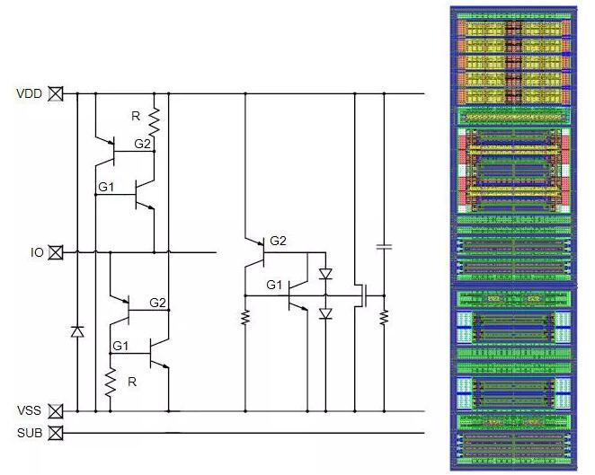
Figure 10: (Example) Packaging of electronic ICs (drivers) on silicon photonics devices using a flip-chip bonding process (?IOP 2016 [11]).
Figure 11: Simplified Tx/output circuit used in silicon photonics SerDes interface.
The 28Gbps interface uses the differential pair concept, as shown in Figure 11. Create a 1V functional circuit using 0.9V core transistors to ensure switching speeds can be achieved. However, these transistors reduce the available ESD design window for Rx, Tx signals to 4V.
Other requirements for ESD protection include low leakage operation and small silicon area.
The ESD protection design includes a complete local protection clamping concept as shown in Figure 12. A 1V supply clamp is integrated to ensure that all stress conditions are handled locally at the interface and the effects of bus resistance are eliminated. The entire clamping structure is isolated from the substrate to reduce noise from the substrate that may originate from digital circuitry located further away on the chip.
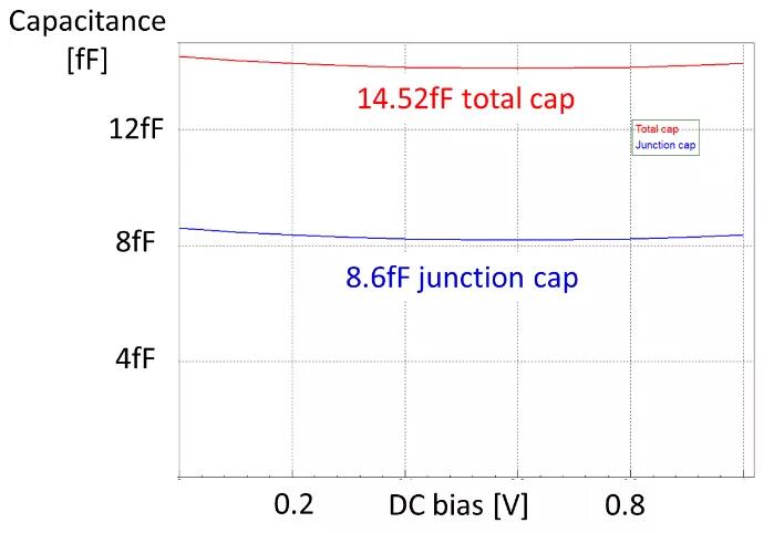
Figure 12: Schematic of a complete local protection method for the Rx and Tx nodes of a SerDes circuit (left). ESD devices based on SCR. An SCR-based 1V power clamp is integrated in the same layout (right). The total area of ESD is 683.75um2.
The total parasitic capacitance on the I/O PAD module consists of different aspects. The junction capacitance can be easily derived from the foundry-supplied Spice model of the diode. The metal connections of the local ESD clamp add significant capacitance. Parasitic metal capacitance can be derived from PEX extraction. Reducing the width of the metal connections reduces the capacitance, but also reduces the stability of the line. The minimum metal width is derived by applying ESD stress to different metals.
When customers require ESD protection using ultra-low capacitance (well below 100fF), the Metal dummy section will be included in the PEX extraction.
Through an iterative process (layout, PEX extraction), the total parasitic capacitance of the ESD clamp circuit was reduced to less than 15fF. The diagram below will show the different steps in this process. The graph below (Figure 13) shows the capacitor value versus the bias voltage on the PAD.
Parasitic capacitance to ground must be reduced to prevent high-frequency signals from shunting to ground.
Equation 1: Capacitive reactance Xc (in ohms) is inversely proportional to signal frequency (f) and capacitance (C)
For high frequencies (>50 Ghz), parasitic capacitance appears as resistance to ground. This impedance must be high enough. A 15 fF capacitor has a resistance of about 200 ohms at 50 GHz.
During the iteration process, in order to reduce the impact of metal connections on parasitic capacitance, some rules were used
-Remove unnecessary via connections
- Reduce metal 1 as much as possible and only place it on top of the connecting diffusion area.
- Prevent metal layer 1 from passing through the junction area.
-Vertical (upwards) connection
Even if the parasitic capacitance is reduced through the above methods, 42% of the parasitic capacitance on advanced nodes is still related to metal connections.
Figure 13: Parasitic capacitance on I/O voltage (total and junction capacitance only).
The local clamping method of Figure 12 was compared with 2 other concepts using transient Spice simulations of HBM ESD stresses
- Concept 1: Proposed local clamping
- Concept 2: I/O PAD module provided by Foundry (dual diode and core power clamp suggested by Foundry)
- Concept 3: Dual Diode and Sofics 1V Core Protection Clamp Combination
From Figure 14 it is clear that Concepts 2 and 3 produce voltage drops much higher than the fault voltage (4V) [12] of sensitive circuits based on thin oxide transistors [12].
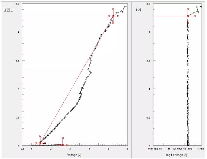
Figure 14: Transient Spice simulation under HBM stress. 3 concepts were compared to verify that the voltage drop on sensitive nodes remains below a maximum of 4V during ESD stress. Only the recommended local clamping can keep ESD stress below 4V. Comparisons were made using 1kV HBM stress and ESD device scaling to 1kV robustness. Simulate the snapback of SCR local clamping using a combined NPN/PNP model.
4. Silicon Photonics 7nm FinFET
To further increase the bandwidth of optical interconnects (beyond 56 Gbps), our customers have adopted TSMC 7nm FinFET technology.
The proposed solution is similar to Figure 12. Two versions of ESD protection were created, one with a parasitic capacitance of 50fF and another with a small capacitance under 15fF. In the paper, these case studies will be included.
Preliminary testing of TSMC’s 7nm FinFET process shows that the ESD local clamping circuit on the SCR has the desired effect (Figure 15).
In 7nm technology, the failure voltage of core transistors (gate to source and drain to source) is about 3V. Fortunately, in many SerDes applications there is more headroom due to other transistors being connected in series (Figure 11). According to the circuit principle, the fault voltage of these circuits is about 4-5V.
7nm ESD clamps have been integrated into 2 designs for high-speed interfaces. At the time of writing, samples of these products are not yet in place, so CDM data is not yet available.
Figure 15: TLP analysis of ESD-on-SCR concept based on TSMC 7nm technology. Protect sensitive core transistors. This reference device for 2kV HBM performance has been scaled down to 15fF and 50fF versions to protect high-speed SerDes.
Summarize
Traditional "dual diode" ESD protection concepts for analog I/O PAD modules have encountered problems protecting high-speed SerDes interfaces in advanced CMOS and FinFET nodes. The total voltage drop across the diodes, bus resistors and power clamps can easily exceed the core transistor's fault voltage. Additionally, "diode up" adds a limiting factor.
This work shows several case studies where the dual diode concept is replaced with a local ESD protection clamp.
I/O PAD module based on proprietary diode triggering and ESD-on-SCR devices. Local clamping reduces bus resistance dependence, lowers clamping voltage, and allows each analog I/O to be optimized individually. Furthermore, these cases show that it is possible to create ESD protection with very low parasitic capacitance and small silicon area.
Data based on dedicated ESD test chips on advanced CMOS and FinFET nodes. The analog I/O in this work is used by more than 20 companies to protect high-speed SerDes interfaces in 28nm CMOS, 16n/12nm and 7nm FinFET technologies.
Disclaimer: This article is reproduced from "IP and SOC Design", which supports the protection of intellectual property rights. Please indicate the original source and author of the reprint. If there is any infringement, please contact us to delete it.
Related Recommendations
Exclusive Interview with Li Gang of Yunfan Ruida: The Precision of Millimeter-Wave Radar Products and the Warmth of Humanity
2026-07-22
2500
RF Passion, Craftsman’s Journey: Over 30 Years of Steadfast Dedication — Interview with Kinghelm Chief Engineer Mr. Qin hongxiang
2026-06-26
2672





 粤公网安备44030002007346号